


Other Parts Discussed in Thread: DRV8256, ,
Hello Team,
We are using DRV8424PPWPR to drive the stepper motor. I have four signals coming from FPGA namely,
1. Enable,
2. Step,
3. PWMIN1
4. PWMIN2.
For this DRV8424PPWPR devie we have four inputs namely,
1. AIN1
2. AIN2
3. BIN1
4. BIN2.
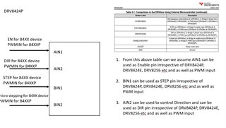
I want to connect four control signals to these four inputs. As DRV8424PPWPR doesn't have separete enable and step inputs, from EVK user guide I got some understadings which are as below. Kindly refer the attached image for more clarity. Let me know if my understanding is correct.
Understandings I had,
1.From this above table can we assume AIN1 can be used as Enable pin irrespective of DRV8424P, DRV8424E, DRV8256 etc and as well as PWM input,
2.BIN1 can be used as STEP pin irrespective of DRV8424P, DRV8424E, DRV8256 etc and as well as PWM input,
3.AIN2 can be used to control Direction and can be used as DIR pin irrespective of DRV8424P, DRV8424E, DRV8256 etc and as well as PWM input.
Regards,
Vikas H
