Hi,
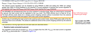
Good Day. Planned to use DRV8962 but is frequency fixed or not? Please confirm. Thank you very much.
Best Regards,
Ray Vincent
This thread has been locked.
If you have a related question, please click the "Ask a related question" button in the top right corner. The newly created question will be automatically linked to this question.
Hi,
Good Day. Planned to use DRV8962 but is frequency fixed or not? Please confirm. Thank you very much.

Best Regards,
Ray Vincent
Hi Ray Vincent,
You are correct. The integrated current regulation loop in the DRV8962 uses fixed tOFF for Itrip current regulation. This alludes to tON being determined by the motor / load characteristics, supply voltage and target current Itrip value. So natively DRV8962 Itrip current regulation is not fixed frequency.
The "another way" described in the data sheet paragraph you outlined in the yellow box mentions an external current regulation method done by using an external controller, for example one can do a cycle-by-cycle control of the input PWM duty cycle using the IPROPIx information from the driver. The algorithm should be developed and run in the controller (MCU). Yes, this could be using a fixed frequency PWM. Keep in mind the regulation loop should be running in the external controller.
Regards, Murugavel
Hi Iam pooja ,
Thanks for posting on behalf of me ,Ray Vincent
Thanks for the support Murugavel,
We need more clarify on the driver usage, requesting you to helps us on this,
we are much confusion state about the driver usage, please help me!!!!
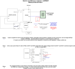
I have attached my requirement and query in attached image, please go through that and let me know if, you required any clarification on this.
Thanks,
Pooja Ak
Hi,
Good Day. When MOSFET will turn, does he need to control INX to handle MOSFET or ENX? Please advise. Thank you very much.
Best Regards,
Ray Vincent
Hi Pooja,
Thanks for getting back with additional information about your application needs. The DRV8962 has four independent half bridges with corresponding IPROPIx proportional current outputs. Each bridge is controlled independently via their corresponding INx inputs. In addition to this the device supports integrated current regulation. The current regulation level for each input can be set as described in the section "7.5.3 Current Regulation" of the datasheet. This will work for inductive loads only. A pure resistive load such as the heater of your application will not work as current threshold will be reached almost immediately at the beginning of tON. So using internal ITRIP regulation is out of question. In order to disable to internal current regulation you'll have input 3.3V to the VREF pin and choose a R-IPROPI such that 3.3V is never achieved at full drive current.
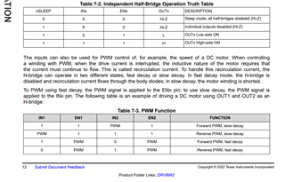
That said you can control the duty cycle of the drive output using INx which will help you achieve variable heating for example. In the block diagram you provided one end of the heater is connected to OUT1 and the other end to OUT2. Let's say we make OUT2 = GND by making EN2 = 1 and IN2 = 0. We can now control the OUT1 side output duty cycle by making EN1 =1 and IN1 = PWM. See bridge control truth table snippet from data sheet below. You may also connect the other heater pin to direct ground. The OUT1 (OUT x) will always swing between VM (24V in your application) and 0V. The output will always be VM when OUT1 = high side conduction. By using principle of duty cycle averaging you can control the heating power. This is a generic method of using PWM where average heating = duty cycle % X heating at 100 % duty cycle. Because of thermal inertia this method works fine in most temperature control systems. This is an open loop method.
You can do a closed loop method by measuring the IRPOPI1 voltage across a suitable set R-IPROPI1. The microcontroller should calculate measurement average over several cycles. Alternatively an external RC can be used from R-IPROPI1 to smooth out the equivalent voltage going to the analog to digital converter input. This might be a better approach for you.
Hi Ray Vincent,
For each half-bridge the corresponding ENx should be 1 for the output to be active, see the truth table in the datasheet. I included the snippet in my reply to Pooja.
Regards, Murugavel
Hi Ray and Murugavel,
Thank you much for your extended support towards my query.
Here by continuing the query and added my understanding,
Please correct me if my understanding is wrong.
Kindly go through the attached image where added my queries .Looking for your support on this.

If I use INX pin ,can I regulate the heater load current ?
Thanks,
Pooja Ak
Hi Pooja,
I'll provide my answers in the same order as your queries in the image snippet you sent. It would be helpful if you could type in your questions directly instead of the image snippet just so I can cut and paste certain portions for context and provide our responses.
1. You are correct. With resistive load internal regulation will not work because of the current rise time which will be almost immediate resulting in narrow current spikes during every regulation cycle. If you disable current regulation by connecting IPROPIx to ground then you won't be able to get current feedback for that channel. Hence I mentioned previously to set VREF at maximum and choose the IPROPIx resistor such that current will never reach the trip threshold. You can ground IPROPIx to disable regulation for sure, but you'll not have current feedback from the internal Isense. You can provide an external current sense resistor if needed.
2. a. If you connect the heater between OUT1 and GND then EN2 or IN2 driving is not necessary. Each half-bridge is independently controlled.
2. b. If you connect the heater between OUT1 and OUT2 you should follow the bridge control truth table I mentioned in my previous reply. OUT2 should be fixed potential, for example low side FET conducting and OUT1 should output PWM based on IN1 frequency and duty cycle.
3. a. During PWM tON output will be 24V (high side FET on) and during tOFF it will be 0V. For example with 10% duty cycle the heater will be active for tON = 10% every PWM cycle. So it will heat up only during 10% ON time which means it will achieve lesser heating compared to tON = 100%. The rate at which heat spreads depends on the thermal mass of the heater and your application system thermal time constant. You can calculate the equivalent current based on the heating achieved like so, (24V/R-heater) x (duty cycle % / 100), in other words average voltage or current. I hope this helps. Your understanding and description about the concept is correct. This is true with any digital bridge control, which is typical of motor driver ICs.
3. b. While this topic is outside the scope of the driver IC support I'd like to point you to useful references. There are plenty of information available in the public domain with topics related to synchronous buck converter design and overview. Here's an example topology. S1 would be the high-side FET and S2 the low-side FET of the DRV8962. Using this approach you can build a voltage or current regulator.
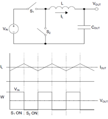
You could also consider other topologies. This application note https://www.ti.com/lit/an/spra873/spra873.pdf might be a good resource for you with regards to LC formulae etc. You won't have to do a complex PID controller but use the concept for control using PWM. Substitute the Peltier element with your heater as they both are resistive.
You could also evaluate these circuits using a DRV8962EVM, www.ti.com/.../DRV8962EVM.
Regards, Murugavel
Dear Murugavel,
Thanks for your feedback,
We received PDRV8962DDWR Samples from TI and started to evaluate the IC with respect our requirement.
Please find the below mentioned details which we carried rework during validation. (We planned to validate the IC by Step by Step; first step is to validate the IC instead of giving PWM we set 1.8 DC to DRV8962, IF it works next step is to provide the PWM but we didn't get the output voltage at PIN (4,5,6)]
1) We set the pin as nSleep=1.8, EN1=1.8 and IN1=1.8 V,but couldn't get the OUPUT Voltage
2) we measured the voltage at pin 1 (VCP), Expected voltage should be 17V which includes the input voltage and internal LDO,
For example, I supplied VM is 12V, means I need to get 12+5 =17 at VCP pin, but we are receiving 12V at VCP.
Kindly helps us on this.
Here By I attached the schematic for your reference.SCHEMATIC FOR DRV8962.pdf
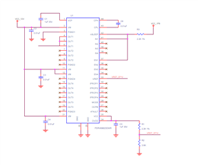
Thanks,
Pooja Ak
Hi Pooja,
The capacitor C6 in your schematic is 0.01uF. It should be 0.1uF, please refer device data sheet table 7-1. Also connect a resistor to ground from IPROPI1 such that the Itrip comparator input will be at a known voltage level with respect to 3.1V VREF in your setup. For example if you connect a 3.3k to ground from IRPOPI1, the output current regulation will not kick in until 4.43A load current (based on the calculation with AIPROPI specification in the data sheet). You can download the EVM schematic from ti.com for your reference.
Regards, Murugavel
Hi Murugavel ,
I appreciate your quick response.
Yes, I have to connect IROP1 to ground. But why I didn't connect means that is Current sense output pin ,moreover I didn't connect any load to IC.
In this case why do I need to regulate or need to set the ITRIP ?
One thing I need to add (After Connecting VREFto IC we observed changes voltage at VCP )
Before that Charge pump was working fine and I got required voltage at VCP but same time I didn't get output voltage .
Please confirm, If I need to get output at(4,5,6)PIn ,do I need to enable nSleep,IN1 and EN1...? this is what my understanding , Is there anything that I need to enable the other pin to get output voltage...?
Voltage variation observed only after connecting VREF by using resistor divider.
Can you please let me know, If I set VREF, IROPI1 to be connected along with this..? if IROPI1 not set, due to over current flow will the IC get damage ?
But I have not connected resistive load right, IC should be capable to support 5A ,then how will it get damage or not getting voltage?
Thanks,
Pooja Ak
Hi Pooja,
It is highly unlikely you may have damaged the driver IC with load never connected unless it was zapped with an ESD or connecting a supply voltage exceeding the specifications. Yes if you want to completely disable regulation and do not want any IPROPI feedback to the MCU you should connect it to ground. In the schematic you sent over the previous message it was floating. If you do need an analog equivalent voltage of the output current an RIPROPIx is needed on IPROPIx and sized such that although regulation is enabled it will never reach the Itrip value thereby never in the zone for regulation. And if IROPI1 was not set, the IC will not be damaged specifically with no load connected or no short circuit in the output. Even in this case internal OCP protection would kick in and protect the IC.
VREF in the schematic is derived from DVDD output from the IC. The load on the pin by the resistors works out to < 1 mA. This should not impact the charge pump. How much was the drop in charge pump voltage? I assume correct value for C6 was used later on, the previous schematic had 0.01 uF.
Yes, you must enable nSLEEP and EN1 for IN1 control to work. IN1 should be high for output HS FET to turn on. See table snippet from the data sheet.

I noticed you have IN1, EN1 and nSLEEP tied to 1.8V via a 2.2K resistor. These three pins have internal pulldown typical value ~200k. The can vary and could be lower. The VIH min spec on these pins is 1.5V and hysteresis 150mV typical. I suspect you may not be exceeding VIH due to the 2.2k series resistor. I recommend bypassing this resistor and tying these pins to 1.8V directly to ensure VIH minimum input on these pins.
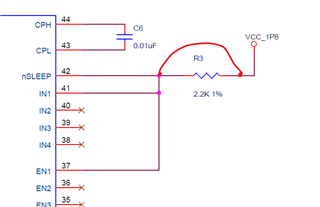
Regards, Murugavel
Dear Murugavel,
Thanks for the support!
Below are the cases which has been carried out during the validation process,
Case 1: After connecting IPROPI (91K) to ground (regulated the current of 200mA), I got voltage as expected at VCP pin and also got output voltage at (4,5,6) pin. (This case I Supplied nsleep ,EN1 and IN1 as 1.8V and also tested with 3.3V )
Case 2: The thing is now, I had given PWM to IN1 pin & supplied 3.3V to nsleep and EN1 but I received DC voltage at 4,5,6 pin instead of receiving PWM.
Case 3: As per the data sheet, IN1 supposed to be powered before VM supplied. Initially EN1, IN1 and nsleep value had been set and supplied voltage at VM Pin (This is the procedure which has been mentioned in the data sheet and same has been followed), In between, with the help of software control, PWM had been disabled at IN1 pin and tested during working condition. Output should have been 0 volt whereas received 12V. i e input voltage)
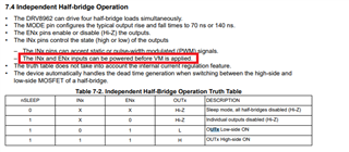
Case4: In continuation, IN1 set for 0 Volt and EN1 and nsleep set for 3.3V then supplied 12V to VM. with this condition, expected results observed.
Case5: EN1 set for PWM(10KHz) and IN1 and nsleep set for 3.3 DC. At this point of time got the PWM output.
By considering the all above cases, results are fine when we set EN1 as PWM. In reality it should be IN1 to PWM. I would request you to help us where do I need to concentrate to get the results with respect to data sheet.
Thanks
Pooja Ak
Hi Pooja,
According to the statement in the data sheet you indicated with a red rectangle it says INx and ENx can be powered before VM is applied. It is not mandatory. In practical situations in an application VM may be active all the time. I just want to make this point clear. You can leave VM active.
See below the half-bridge operation truth table from the data sheet. As per this table when EN1 = 1 and IN1 PWM = low, OUT1 low side will be on and it will read 0V with respect to ground, When EN1 =1 and IN1 PWM = high, OUT1 high side will be on and it will read VM voltage with respect to ground. Note internal current sensing is in the high side of the half-bridge only. In order to realize current regulation load must be connected between OUTx and ground.

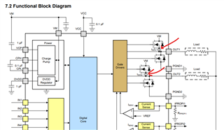
See below scope capture EN = 1, IN1 = 25% PWM pink trace between IN1 and GND, OUT1 yellow trace between OUT1 and GND. I do not see any issues with the described behavior of the half-bridge.
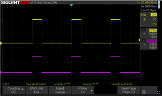
Regards, Murugavel
Also I want to add, while providing PWM input to EN1 with IN1 = 1 you will observe PWM output at OUT1. However during PWM low EN1 will be 0 which will make output HiZ during this low time. If there is stored indictive energy in the load this will not be a desirable situation for example with a spinning DC motor load. The application must use ENx as enable only and INx as input / PWM. It should work as per the half-bridge truth table in the datasheet.
Regards, Murugavel
Dear Murugavel,
Please look over the details below about the validation we did today.
1) As you suggested, we connected resistive load to the OUT1(4,5 and 6), still receiving DC in output side . [[In this scenario, NSLEEP=3.3V, EN1=3.3V, and IN1=PWM were given.]
2) IN2,IN3,IN4,EN2,EN3,EN4,IPROP2,IPROP3,IPROP4,PGND2,PGND3,PGND4,MODE ,OCPM these pins are in the floating state, any reason behind this to not get PWM OUTPUT??
3)I've captured the image during different working condition.
Please assist me in determining where I need to make changes.

Violet is IN1-3.6V,PWM
GREEN: OUT1 -5V
BLUE: EN1-3.6
YELLOW: NSLEEP-3.6
VIOLET is IN1-3.6V]
GREEN EN1 -PWM INPUT 3.6V 10KHz
BLUE OUT1 -PWM OUTPUT (5V ) 10KHz
YELLOW: NSLEEP 3.6V DC
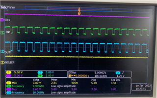
Thanks,
Pooja Ak
Hi Pooja,
I'm unable to reproduce the issue you are experiencing. Could you please double check the schematic and the circuit board you have? Do you happen to have one of our DRV8962EVM to compare? If not I recommend you order one of this EVM for evaluation and comparison. Can you perform and compare this same test with another DRV8962 sample using your PCB?
Leaving IN2,IN3,IN4,EN2,EN3,EN4,IPROP2,IPROP3,IPROP4,MODE and OCPM pins in floating state while you are working with only IN1 channel is fine. However for best practice I'd suggest you connect PGND2,PGND3,PGND4 to ground along with PGND1.
In both images you sent VM DC as well as VM PWM is shown as 5V. However the reference schematic I received shows VM = VCC_12, I assume 12V. Did you use VM = 5V for testing? Can you also do waveforms capture with no load connected? Can you also connect a 10k pull-up resistor from nFAULT to DVDD and check the status of the nFAULT pin to see whether a fault condition exists during your tests? Thanks.
Regards, Murugavel
Hey Murugavel,
Thank you so much for your extending support,
1) I have verified at fault pin, we observed low voltage and by replacing the new IC, got PWM output.
TI ----In both images you sent VM DC as well as VM PWM is shown as 5V. However the reference schematic I received shows VM = VCC_12, I assume 12V. Did you use VM = 5V for testing?
Waveform image which was shared to you was having input voltage of 5V, yes, for testing purpose input voltage varied from 5 to 25.
Still validation is in progress, I will update you .
Thanks,
Pooja Ak
Hi Ray Vincent,
Can you please go ahead and close this thread. Looks like the original issue has been resolved and Pooja is doing further evaluation of the product. Should there be any other questions in the future let's open a new thread. Thanks.
Regards, Murugavel
Dear Ray & Murugavel
Thank you so much for the support !
I apologies' for the delay; I became distracted by another project,
Related to the DRV8962 IC we got PWM output and we set the ITRIP current.
Today, we began the process of further validation. Like integrated with ADC and Thermistor .
please clarify me ,If I need suggestion regarding the further validation ,shall I create another Issues ?
Thanks,
Pooja Ak
Hi Pooja,
Thank you for the update and confirming the issue mentioned in the post was resolved and the driver works as expected. For future new support request you are welcome to create a new thread. Kindly update this thread status to "CLOSED". Thank you.
Regards, Murugavel