Hi expert,
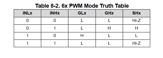
Q1:
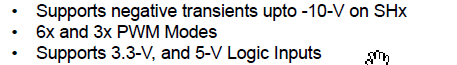
I am using DRV8329 for BLDC motor control. I have noticed that DRV8329 support 3xPWM control mode, which is described in datasheet:
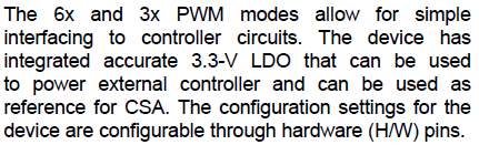
However, I don't find any hardware pin number to settle it PWM mode. Can you give me some suggestions?
Q2:
Meanwhile, I have further question about DRV8329 usage, I have done double test for PWM generation:
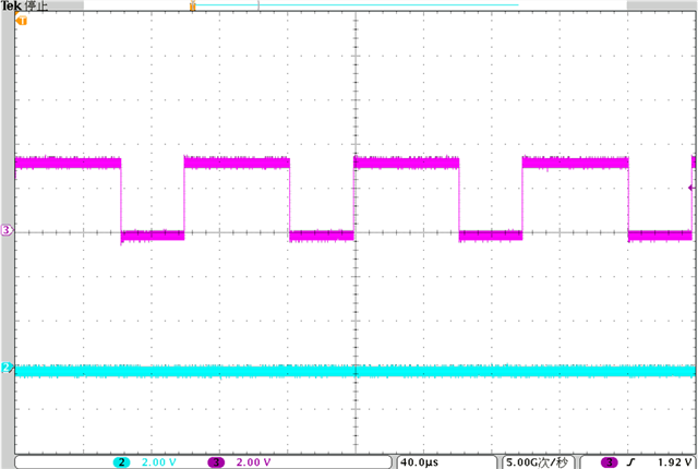
P0-Normal
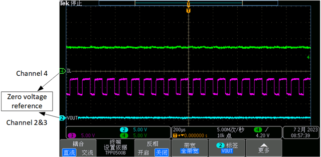
Background: Connected power supply pin, set INHA & INLA on with PWM, then measure OUTA voltage.
Phenomenon:
Gate driver:
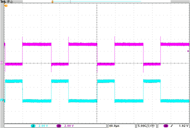
OUTA:
nFAULT: ~2.5V. For this situation, the voltage of nFAULT signal is not closed to AVDD, which is 3.3V. Is it normal?
Update: I check its voltage (with and without MCU pin, which is used to read nFAULT voltage), and it is related to MCU pin input resistor, so it should be normal.

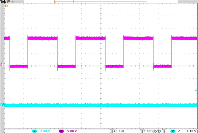
P1-Abnormal
Background: Connected power supply pin, set INHA on with PWM and INLA off, then measure OUTA voltage.
Phenomenon:
Gate driver:
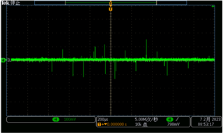
OUTA:
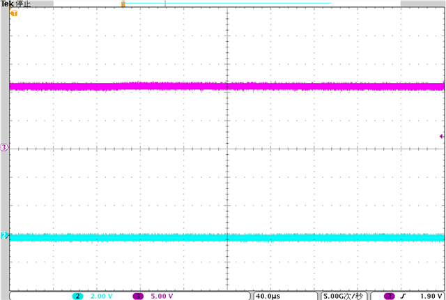
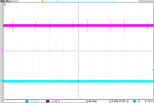
nFAULT: ~0V. Fault happens. What causes fault, no current circuit added?
Do you have any suggestions about this phenomenon?
Best Regards
Sal


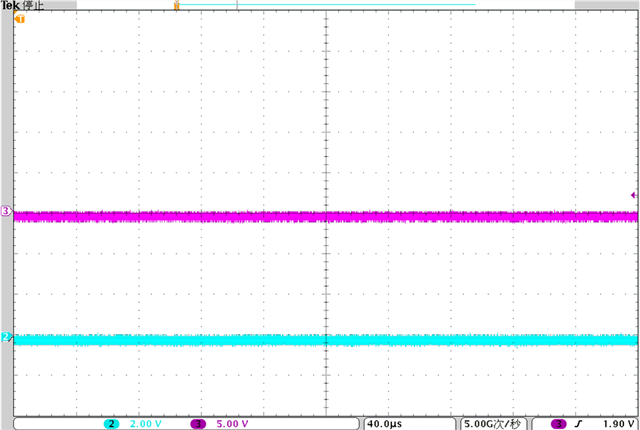
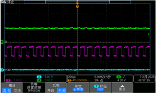 (Green is OUTA; pink is GHA; blue is GLA; all connected to GND)
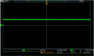
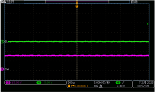 (Green is High-side: PVDD->SHx)