This thread has been locked.

If you have a related question, please click the "Ask a related question" button in the top right corner. The newly created question will be automatically linked to this question.

DRV8711: DRV8711 DRV8711 Stepper Drive Reg Read Issue continuity

Part Number: DRV8711
Other Parts Discussed in Thread: TM4C1294NCPDT

Sir.,

I apologize for the late reply. This query is the continuity for DRV8711: DRV8711 Stepper Drive Reg Read Issue.


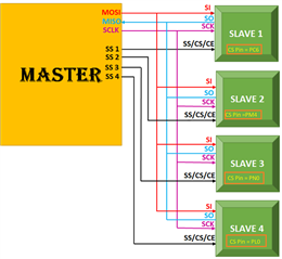
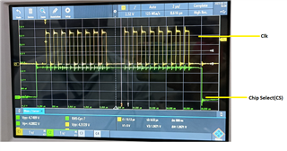
And the last question you asked , Each device has it's own dedicated chip select (CS) signal. Is the correct CS signal is used to read to the desired driver?

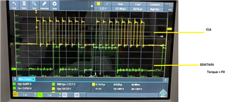
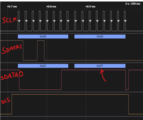
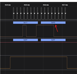
Yes Each device has its own dedicated CS signal. But read will be done on 5th attempt only. Kindly resolve this issue as soon as possible. 


  • Hi Tom,

    Let me look into your question and I will get back to you within 24 hours.

    Regards,

    Pablo Armet

  • Please Take your time and do the needful.

    Thank you

  • Hi Tom,

    When attempting to read one device. Only one CS signal is used correct. Meaning the CS chip corresponding to the chip being read will be set/unset for 5 times until the updated values are read correctly?

    Regards,

    Pablo Armet

  • Hi.,

    Thank you for your prompt response. we are using 4 stepper motors and 4 DRV 8711 Driver IC. In the below diagram i explained about each motor has each chip select(CS) pin.this individual CS pins connected into the Micro controller.

    For your reference

     SPI_LSU_SuctionArm_Motor_CS_High GPIOPinWrite(GPIO_PORTC_BASE, GPIO_PIN_6, GPIO_PIN_6);
     SPI_LSU_Economizer_Motor_CS_High GPIOPinWrite(GPIO_PORTM_BASE, GPIO_PIN_4, GPIO_PIN_4);
     SPI_RSU_SuctionArm_Motor_CS_High GPIOPinWrite(GPIO_PORTN_BASE, GPIO_PIN_0, GPIO_PIN_0);
     SPI_RSU_Economizer_Motor_CS_High GPIOPinWrite(GPIO_PORTL_BASE, GPIO_PIN_0, GPIO_PIN_0);

    I connected Individual CS pin Please let me know how to read data in single attempt. Thanks in advance.

  • Hi Tom,

    Thank you for the information. I would add some delay between each SPI write and read function. start with ~5us for settling time. 

    Regards,

    Pablo Armet

  • Hi.,

    Thanks for your response. I tried as per your above idea but i didn't seen any changes. Please ensure my code for read the data in first attempt.

    Write Sequence:

    void SPI_DRV8711_Write(unsigned char dataHi, unsigned char dataLo)
    {
    switch(Stepper_Motor_NodeId)
    {
    case 1:
    g_Write_Data01[0] = dataHi;
    g_Write_Data01[1] = dataLo;
    SPI_Motor1_CS_High;

     SysCtlDelay(500);//5us
    SSIDataPut(SSI2_BASE, dataHi);
    while(SSIBusy(SSI2_BASE));
    SSIDataPut(SSI2_BASE, dataLo);
    while(SSIBusy(SSI2_BASE));
    Motor1_CS_Low;
    break;

    case 2 to case 4 remaining motor sequence (Motor 1,Motor 2,Motor 3) is same as case 1.

    Read Sequence:

    unsigned int SPI_DRV8711_Read(unsigned char dataHi, unsigned char dataLo)

    Read_Data = 0;
    SPIMotor1_CS_High; 

    SysCtlDelay(500);//5us

    SSIDataPut(SSI2_BASE, dataHi);
    while(SSIBusy(SSI2_BASE));
    SSIDataGet(SSI2_BASE, &RxdataHi);
    SSIDataPut(SSI2_BASE, dataLo);
    while(SSIBusy(SSI2_BASE));
    SSIDataGet(SSI2_BASE, &RxdataLo);
    g_Read_Data01[0] = 0x80 ^ RxdataLo;
    g_Read_Data01[1] = RxdataHi;
    Motor1_CS_Low;
    break;

    case 2 to case 4 remaining motor sequence(Motor 1,Motor 2,Motor 3) is same as case 1.

    If you need any information let me know.

    Thanks You

  • Kindly reply as soon as possible 

    Thank you

  • Tom,

    Pablo is out of the office today.  Let me check with someone else on the team that can help here.

    Regards,

    Ryan

  • Hi Tom,

    This looks like an issue with the external controller SPI configuration. Perhaps the clock polarity or phase does not match with the device requirements? Do you happen to have the SPI signal waveforms showing the read operation of all the five packets. As well as do you use a logic analyzer such as Saleae to probe the SPI packets? Thanks.

    Regards, Murugavel 

  • Hi Tom,

    Please also confirm proper pull-up resistor had been provisioned on the SDATO pin, as mentioned in the datasheet this is an open drain output pin. Would it be possible to share with us the schematic diagram of the multiple drivers to MCU SPI connections? Thanks.

    Regards, Murugavel

  • Hi Murugavel.,

    Thank you for your immediate response. Here by i attached schematic for our DRV8711. The pins are connect correctly. And dalso i include scope result for clock and data.

    Data will be generated after 4 clock pulses sowe read the data in 4th attempt.Kindly resolve this issue.

    Thank you

  • Hi Tom,

    Thank you for providing the information. In the schematic I do not see a pullup resistor on the SDATO pin of the DRV8711. Could you please confirm a pullup is provided on this pin? What is the value of this resistor?

    I'd like to see all the failing data packets as well as the successfully read data packet at the 4th attempt. I also need all the four signals SCS, SDATI, SDATO and SCLK for diagnosis. Thank you.

    Regards, Murugavel

  • Dear Murugavel.,

    Thank you.

    I attached schematic for your reference.This TM4C1294NCPDT controller. WE connect the 1k pullup resister in microcontroller(SPI Data In ) to SDATAO pin in drv8711.I'm sure we didn't connect any pull up in (SPI Data Out) to SDATAIn pin in drv8711. 

    SCS, SDATI, SDATO and SCLK Scope diagram i will post soon.

    Thank you

  • Hello Tom,

    Thank you for the information. Could you also please confirm VREFA+ is in the same 3.3 V domain? I assume it is. Pullup is needed only for the SDATAO pin of the DRV8711 SPI circuit. While you get the scope diagram I'm wondering if you happen to have a SPI diagnostic tool such as the Saleae? If you have it you can save the .sal file, zip it and share it with me. This will be more helpful with diagnosis. 

    Regards, Murugavel  

  • Hi Murugavel.,

    Yeah i'm sure   VREF+ is 3.3v . I attached scope images for sclk,CS,SdataIn, SdataOut for your reference.

       Stepper_Motor_Torque_Register.TORQUE   = 0xF0;

    Kindly help me what is reason behind the mystery for reading 4th attempt.

    Thank you

  • Hello Tom,

    Based on the waveforms it appears the MCU SSI configuration does not match with the DRV8711 SPI format. Please confirm if your scope shots were for a write operation. During a write operation (MSB logic low) SDATAO will stay high. I'm not sure if this was what you observed. The scope capture does show some activity on the SDATAO. I'm not sure if this happened during a write or a read operation. Please clarify.

    I have an DRV8711 EVM setup and I tried to replicate the same write operation as your test case, TORQUE register = 0xF0 from its default value of 0xFF. 

    Here's first read of the TORQUE register to confirm the default setting was indeed 0xFF.

    I followed this read with a write operation to this register with SDATAI value = 0xF0. See snippet below. Note the sequence of the channels are same as the previous snippet for signal labels. Also note SDATA0 was high during the write operation.

    I did an immediate single read of the TORQUE register. See snippet below. The newly written value was read and displayed correctly in the first attempt. This confirmed a write was executed as expected as well as a read operation.

    I am unable to reproduce what you're experiencing with the MCU in your system. Please verify the SPI (SSI) configuration of your MCU. This issue points to a SSI configuration issue of the MCU in your system. 

    For clarity I will state my observations on the MCU data packet scope shots you sent in a separate reply. 

    Regards, Murugavel

  • Hello Tom,

    Based on the below snippet from one of your scope captures - see snippet below - the SDATAO line did not go high for a while after the clocks and SCS based on the other capture you had. It would be useful for diagnosis to have SCS along with these two channels. If it is not possible just the SCS and SDATAO. Regardless this points to an SSI configuration issue of the MCU SPI peripheral.

    Ideally I'd like to get a four channel capture for a write operation and read operation separately. The issue you have appears to be MCU configuration related. You may want to contact MCU support E2E if you're unable to find the correct configuration. Meanwhile I'll be happy to answer any question you may have with the DRV8711 device and its SPI communication. Thanks.

    Please make sure the configuration matches with the data sheet requirements, see page-27 of . https://www.ti.com/lit/ds/symlink/drv8711.pdf . 

    Regards, Murugavel

  • Dear Murugavel.,

    Thank you for your valuable response.We have a experimental for your above instruction.i attached read write values for your reference.

    And also please ensure below read /write code is Right?

    SysCtlPeripheralEnable(SYSCTL_PERIPH_SSI2);
    SysCtlPeripheralEnable(SYSCTL_PERIPH_GPIOD);
    GPIOPinConfigure(GPIO_PD3_SSI2CLK);
    //GPIOPinConfigure(GPIO_PD2_SSI2FSS);
    GPIOPinConfigure(GPIO_PD1_SSI2XDAT0);
    GPIOPinConfigure(GPIO_PD0_SSI2XDAT1);
    GPIOPinTypeSSI(GPIO_PORTD_BASE,GPIO_PIN_0 | GPIO_PIN_1 | GPIO_PIN_3);
    SSIConfigSetExpClk(SSI2_BASE, g_ui32SysClkFreq, SSI_FRF_MOTO_MODE_0,SSI_MODE_MASTER,500000,8);

    SSIEnable(SSI2_BASE);

  • Hello Tom,

    Thank you. I'm not sure I follow the table you posted. It appears the first two rows were SDATAI to TORQUE register. What is the third row? Assuming it was the SDATAO during the read indicated in the 2nd row, clearly the write operation was not done correctly. This is what I mentioned in my previous reply that there appears to be a protocol issue. The only way to verify the protocol by looking at the four channels simultaneously. Would it be possible to provide this information for each of the rows in the table? 

    Unfortunately I am not familiar with the macro functions of your code. I'll try to understand it as best as I could and give you a feedback. For in depth review of your macro code you'll have to raise an E2E support in the Microcontrollers forum.  

    In the configuration macro, I did notice you were configuring the SSI to SSI_FRF_MOTO_MODE_0. Based on the device description in its user's guide (UG) "When the SPH phase control bit is clear, data is captured on the first clock edge transition. If the SPH bit is set, data is captured on the second clock edge transition.". Looks like MODE_0 is not the correct mode to interface with the DRV8711. You should use the mode which has SPH bit set such that data is captured on the second clock edge. I'm not 100% sure if it is called as SSI_FRF_MOTO_MODE_1 in the macro of this MCU. Please verify. In essence you should use the mode that has SPO = 0 and SPH =1. " Freescale SPI Frame Format with SPO=0 and SPH=1.". Please try with this setting. It should resolve your issue. Let us know if it works. Thanks.

    Regards, Murugavel

  • Hi Tom,

    I hope you were able to make this firmware change with MCU SSI configuration and resolve the issue. If so, please update the status of this thread to "Closed". Thank you.

    Regards, Murugavel

  • Thanks for your Support.

    Actually we didint have possible to show all the 4 pins in single scope. And i tried all you said in above queries,still i don''t know what drv parameter tuning for single read.

    I have one lst opinion for you,here by i attached the write and read sequence in my application logic.Please ensure this for my reference.

    case 0://Motor Current
    if((Motor.Stall==1)&&(Motor.Fault==1))  
    {
    if(Start==1)
    {
    Stepper_Motor_NodeId = 1;
    Motor_Torque_Register.TORQUE = 0xF0;
    Motor.Write_Cmplt = 0;                                                 // when the write was complete
    Motor.Write = 1;             
    while(!(g_Cal_LSU_SuctionArm_Motor.Write_Cmplt))   // if the write was not complete 
    {
    g_Stepper_Motor_NodeId = 1;
    if(Read_Data01[01]==Motor_Torque_Register.TORQUE)  // write data and torque will be same
    {
    Motor.Write_Cmplt=1;                                                     // Write data is completed
    }
    else
    {
    Motor_Current_WriteSequenece();                                 // write sequence is already uploaded
    }

    }
    Motor.Write_Cmplt_Fault = 0;
    Stepper_Motor_NodeId = 0;
    Motor.Hold_Sequnece = Stop;
    Motor.SetSpeed = Speed;
    SetPluses = MotorDegree;
    Motor_Pulse_Calculation();
    Motor.Sequnece_No = 1;
    }
    }
    else
    {
    ....}
    break;

  • Hello Tom,

    Thanks for the update. I did understand the constraints you had getting all four channels, really appreciate you providing all the requested captures. I tried to identify the root cause for your issue from the captures you sent.. The DRV8711 is designed to respond to a single correct SPI write or read. There is no tuning required for the SPI timing, all is required is to match the published timing requirements. I tried this in my setup and verified to be the case. We use an MSP430 in our EVMs which is a different MCU compared to the TM4C1294NCPDT MCU you are using. I am not familiar with its SSI SPI mode settings which is why I recommended to have a E2E support thread with the Microcontroller team. One last thing I could think of is to slow down the SPI clock frequency to 1 MHz or 500 kHz and see if you have successful write and read in one attempt.   

    If I understood correctly you've implemented a workaround for the issue with your code which will make multiple write sequence attempts until the read value matches the written value. This could be a logical fix assuming you were able to successfully write/read verify values within a few cycles of write and read all the time. My concern would be, what if you were stuck in the while loop under varying operating conditions such as temperature and supply voltage changes. I'd prefer you have a solution to successfully write and read DRV8711 registers with one SPI write or read operation. If not, for this workaround you have, perhaps, implement an exit from the loop if the write/read attempts exceed a fixed number of attempts let's say 5 and flag an error condition. 

    Regards, Murugavel   . 

  • I need microcontroller expert. Thankyou so much for your valuable support Murugavel

  • Thank you Tom. I specialize in stepper motor drivers at TI. We have dedicated support group for Microcontrollers and within that group specific engineers to support the TM4C1294NCPDT MCU..I hope you'd get this resolved.

    Regards, Murugavel