This thread has been locked.

If you have a related question, please click the "Ask a related question" button in the top right corner. The newly created question will be automatically linked to this question.

Layout of gate traces

Other Parts Discussed in Thread: OPA607, DRV8301, DRV8300

Hello Ti,

I have a question about of the layout from Gate-Traces. I’ve found a rough estimation formula to calculate the inductance of broad- and edge-coupled traces:

It’s clearly to see that the inductance of the broad coupled (option 2) traces are much smaller. But I’ve never seen a PCB layout that uses broad coupled traces, why is this so?

The only reason I can think of would be that the gate traces are so short that it doesn’t make a huge difference. But with longer traces (a few centimeters) that would make a difference.  

The other reason I can think of would be that it's very impractical to route the gate trace in broad coupled form because for example in this layout below, I need the top and bottom layer as power planes (PVDD, GND) (and other things). I think I can’t put a power layer in an inner layer because of the heat distribution.


Are these the reasons or are there other things to consider?

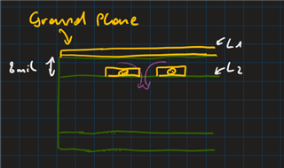
What would happen to the inductance of the gate traces, when they are for example on layer2 and on the top layer is a ground plane? (like in the picture below) If it is changing the inductance, is there then a difference for the low-side and high-side fet gate traces?


Do you know a book where something like this is discussed?

Thanks in advance,
Daniel

  • Hi Daniel,

    Thank you for your question. Could you put TI product name for this question?

    regards

    Shinya

  • Hello Shinya,

    of course, in this Layout the DRV8301 is used because the DRV8300 wasn't available a few months ago. In future designs the DRV8300 will be used. The MCU is the F28069m (will be replaced by the 25c,49c or 39c in future), OPA607 for current sensing.

    Best regards,
    Daniel

  • Hi Daniel,

    Thank you. This device is supported by different group. I send note to them. Please wait their response

    regards

    Shinya Morita

  • Thank you Shinya!
    Best Regards, Daniel

  • Hi Daniel,

    The following Application Note details the PCB layout considerations needed for motor drive systems:

    Section 4 discusses general routing techniques regarding gate traces such as the need to make them as wide and short in length as possible. This helps to minimize inductance, loop area, and the possibility of noise caused by dv/dt switching.

    I would recommend looking over the App Note to learn about other/additional practices to observe in order to optimize your layout.

    Best,

    ~Alicia

  • Hi Daniel,

    I need the top and bottom layer as power planes (PVDD, GND) (and other things). I think I can’t put a power layer in an inner layer because of the heat distribution.

    Personally I prefer to have the power planes VM and GND to be the inner layer next to each other for better coupling capacitance created by the 2 copper layers. For heat dissipation for the power FETs, I would have larger area of copper around the FET Drain pads and connected to the VM layer with many vias. 

    Brian 

  • Hello Alicia,

    thank you for your answer. I’ve already read this document several times. I know the standard routing for gate traces but I wanted to ask, why I’ve never seen broad coupled gate traces, where the inductance would be much smaller for longer traces. And if a reference plane would affect the inductance of the edge coupled traces and if yes how.

    I tried to find books/references about it in the standard pcb design books, but I didn’t find any about this specific case.

    Best regards,
    Daniel

  • Hello Brian,

    thanks for your tip. I also heard about that with the coupling capacitance, but I thought in my case where I have sometimes 60A on 2oz copper it could get very hot. And when using a calculator for the width, I got for the inner layer three times the width compared to outer layers. Therefore, I used the outer layers. The fets that I use in this layout are TO-220 with an heatsink.


    When you say inner layer for VM and GND is there than the pcb core between? Or do you mean that one power plane is on an inner layer and the other power plane is on an outer layer?

    Because where I buy my pcb boards the manufacturer creates it like that:

    TOP (Layer 1)

    Prepreg = 8mil

    Layer 2

    Core 40mil

    Layer 3

    Prepreg = 8 mil

    BOTTOM (Layer 4)


    I think the coupling capacitance should be more effective when TOP and Layer 2 or Layer 3 and BOTTOM is used, or do I miss something here?

    Best regards,
    Daniel

  • Hi Daniel,

    Thank you for the clarification. I will aim to provide a response soon.

    Best,

    ~Alicia

  • Hi Daniel,

    I also heard about that with the coupling capacitance, but I thought in my case where I have sometimes 60A on 2oz copper it could get very hot. And when using a calculator for the width, I got for the inner layer three times the width compared to outer layers. Therefore, I used the outer layers. The fets that I use in this layout are TO-220 with an heatsink.

    I didn't know yours running at 60A motor current -- serious stuff. At this high current, sure the heat dissipation is higher priority than layer-to-layer coupling capacitive. In this case, it makes sense to have the power and ground planes on the outside layer for cooling. 

    To maximize coupling capacitance, I specified minimum thickness for the core. 

    Brian

  • Hey Alicia, I think you suggested this as an answer because it also relates to my question in a certain way.

    I know it's more of a theoretical question, but a few more words (or some references) would have been nice, but doesn't matter.

    A few days ago a friend of mine told me that he saw once a board with broad coupled gate traces. They tried it first with edge coupled, but that didn't work in their case. Unfortunately I don't know more details.

    Best regards,
    Daniel