This thread has been locked.

If you have a related question, please click the "Ask a related question" button in the top right corner. The newly created question will be automatically linked to this question.

DRV8311: SPI implementation, code interpretation

Genius 17695 points
Part Number: DRV8311

Hi Experts,

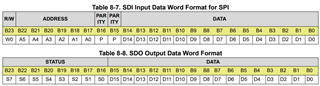
We have some question regarding drv8311.c library (from TI). In the lines 534 to 538 you read SPI values. We cannot understand, why you do this concatenation of readword1 and readword2. We would expect to find the desired data exclusively in readword2. Can you please explain the process a little more? How often do we have to read the SDO data to have the correct answer of the DRV8311?

    // Read the word
    readWord = SPI_readDataNonBlocking(obj->spiHandle);
    readWord1 = SPI_readDataNonBlocking(obj->spiHandle);
    readWord2 = SPI_readDataNonBlocking(obj->spiHandle);
    readWord = ((readWord1 & 0xFF) << 8) | (readWord2 & 0xFF); //concatenate D14:D0 

The second question is about the parity bit calculation in drv8311.h (from TI). At the lines 1254 to 1270 you calculate the parity bit. It seems, that the read or write bit does not count for calculating the parity bit. Is this correct? So for reading the parity is always uneven and for writing the parity is always even? 

static inline DRV8311_Word_t DRV8311_buildCtrlHeader(
                                            const DRV8311_CtrlMode_e ctrlMode,
                                            const DRV8311_Address_e regAddr)
{
    uint16_t parity = 0;
    uint16_t temp = regAddr; 

    while(temp)
    {
        parity ^= (temp & 1);
        temp >>= 1;
    }

    DRV8311_Word_t ctrlHeader = ctrlMode | (regAddr) | (parity & 1); 

    return(ctrlHeader);
} // end of DRV8311_buildHeader() function

Thank you.

Regards,
Archie A.

  • Hi Archie,

    Thank you for posting to the Motor Driver's forum!

    Unfortunately, I did not get the chance to look at this today, and will aim to provide a response shortly.

    Best,

    ~Alicia

  • Hello Alicia,

    Thank you, looking forward to hear an update.

    Another question arose, while Cx was studying the datasheet of the DRV8311S. What is the correct sequence to start the BLDC motor using the PWM Generation Mode? We want to use the DRV8311S in this mode. We also want to use the PWM_OSC_SYNC = 7h setting, where the SPI clock is used for the DRV8311 internal system oscillator. What is the correct sequence to have a turning motor at the end? Do we have to connect the SPI clock to INLB/PWM_SYNC of the DRV8311 or is this not necessary?

    Regards,
    Archie A.

  • Hi Archie,

    Regarding the first question about why the concatenation of readword1 and readword2 occurs, this happens because readword1 is reading in data bits D14:D8 and readword2 is reading in data bits D7:D0 of the register that is getting read. readword1 and readword2 are then concatenated together to give the full value of the register. For more information about how the SPI read sequence of this device works, please see page 48 of the datasheet, section SPI Read Sequence.

    It seems, that the read or write bit does not count for calculating the parity bit. Is this correct?

    Yes, this is correct.

    Regarding the most recent question, if the DRV8311S is being used in PWM Generation mode, then the PWM_SYNC signal from the MCU to the INLB pin of DRV8311S will need to be connected.

    Best,

    ~Alicia

  • Hello Alicia,

    Thank you very much for the fast response. We have this query also:

    Another question arose, while I was studying the datasheet of the DRV8311S. What is the correct sequence to start the BLDC motor using the PWM Generation Mode? I want to use the DRV8311S in this mode. I also want to use the PWM_OSC_SYNC = 7h setting, where the SPI clock is used for the DRV8311 internal system oscillator. What is the correct sequence to have a turning motor at the end? Do I have to connect the SPI clock to INLB/PWM_SYNC of the DRV8311 or is this not necessary?

    Can you please clarify the correct programming sequence/steps for having a turning motor with this setting mentioned in the question above?

    Thank you.

    73,
    Archie A.

  • Hi Archie,

    Thanks for the question! Today is a TI holiday, we will aim to provide a response by the end of the week.

    Regards,

    Anthony 

  • Hi Archie, 

    To clarify, as the DRV8311S is not currently available, did you mean to refer to the DRV8311P (tSPI) variant instead?

    Best,

    ~Alicia

  • Hello Alicia,

    Thank you for clarifying.

    Customer is asking about the DRV8311S. Either way for DRV8311P, hoping to clarify us the correct sequence of programming as described for SPI variants.

    Regards,
    Archie A.

  • Hi Experts/Alicia,

    Any update? Customer also said that they have samples of DRV8311S. Got some samples of the DRV8311S last year, but had to do other projects in between. They are using the DRV8311S.

    Thank you.

    Regards,
    Archie A.

  • Hi Archie,

    I will aim to provide a response by the end of Wednesday next week.

    Best,

    ~Alicia

  • Hi Archie,

    Thank you for your patience.

    To use PWM Generation mode, you will need to make sure that PWM_CTRL1 -> PWM_Mode = 0x3 and PWMG_CTRL -> PWM_OSC_SYNC = 0x7. Section 8.3.2.3 PWM Generation Mode (DRV8311S and DRV8311P Variants) of the datasheet goes into more details about other register configurations that will need to be considered for PWM Generation mode.

    programming sequence/steps for having a turning motor

    To have a turning motor, what you would need to do is update the following register iteratively based on whatever commutation is desired/needed to spin the motor:

    Best,

    ~Alicia

  • Hi Archie,

    Please click "Resolved" to let us know if your question has been resolved. Closing the thread for now.

    Best,

    ~Alicia

  • Hello Alicia,

    I've been asking an update from Cx, been told that they'll get back to check on this once they have further queries.

    Yes, seems that this solved already.

    Thank you,
    Archie A.

  • Hi Alicia,

    Apology. We still need your assistance:

    Cx still have issues with the register settings. The SPI communication seems to be established and I when compare the SPI signal from the launch pad (using a logic analyzer) to the SPI signals I programmed, then they look the same. So far I feel that the SPI communication is working properly.

    However, when I try to write to a register, the driver then immediately switches into the Fault state. What am I missing? Also can you please tell me which registers I can set, using the launch pad and your instaspin software, to have a turning motor? What I could see, is, that the launchpad generates PWM signals to turn the motor. How can I set the registers, using instaspin, to have the drv8311 using its internal PWM generation mode?

    Thank you.

    Regards,
    Archie A.

  • Hi Archie,

    However, when I try to write to a register, the driver then immediately switches into the Fault state. What am I missing?

    Just to verify, the following format, shown below, is being observed for the SPI communication, correct?

    when I try to write to a register, the driver then immediately switches into the Fault state

    To clarify, is the fault state that is being triggered the SPI_FLT? If so, the condition that  triggers an SPI_FLT is either a fault in the SCLK or the address, as shown below, so I would recommend verifying that those are correct.

    How can I set the registers, using instaspin, to have the drv8311 using its internal PWM generation mode?

    To clarify, are you are wanting the use the DRV8311xEVM InstaSPIN_Universal_GUI? If so, please see the following from the user's guide:

    Best,

    ~Alicia