This thread has been locked.

If you have a related question, please click the "Ask a related question" button in the top right corner. The newly created question will be automatically linked to this question.

DRV2667: VDD MIN

Part Number: DRV2667
Other Parts Discussed in Thread: DRV2665

Dear Technical Support Team,

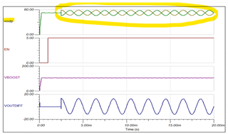
According to the revision E,• Changed VDD MIN spec from 3.0 to 3.3.

What kind of effect will it have on the operation if it is used from 3V to 3.3V?

My supply voltage for VDD is 3.3V within recommendation.

But it's no margin about noise.

Best Regards,

ttd

  • Hi ttd,

    We changed the minimum to 3.3V since below 3.3V there is significant risk that the device will stop working/shutdown. The amount of risk is device-to-device so we can only guarantee that VDD will operate correctly with a minimum of 3.3V.

    Best regards,

    Jeff McPherson

  • Hi Jeff,

    Thank you for your reply.

    What is the recommended voltage for VDD?

    Datasheet spec is defined with VDD=3.6V. On the other hand, general interface such as I2C is VDD=3.3V for FPGA and CPU etc.

    Best Regards,

    ttd

  • Hi Jeff,

    Since the DRV2667 is a type of boost converter that repeatedly turns on and off until it detects an overcurrent and then boosts the voltage to the set value, I don't think it is related to Vin. Is it correct?

    Also, since the operating voltage of the boost converter is generated by a charge pump, is there any possibility that it will not rise to the expected voltage if it is too low?

    Which part of the boost, the Charge pump, or the Digital Engine is affected?


    Best Regards,

    ttd

  • Hi ttd,

    Since the DRV2667 is a type of boost converter that repeatedly turns on and off until it detects an overcurrent and then boosts the voltage to the set value, I don't think it is related to Vin. Is it correct?

    I don't think I understand this question. Can you rephrase or elaborate?

    What is the recommended voltage for VDD?

    Datasheet spec is defined with VDD=3.6V. On the other hand, general interface such as I2C is VDD=3.3V for FPGA and CPU etc.

    VDD has no typical value listed, so the recommendation is just 3.3V<VDD<5.5V. VDD = 3.6V would be a good case to use since it would match the electrical characteristics table. I understand the strict 3.3V minimum makes things more difficult.

    Also, since the operating voltage of the boost converter is generated by a charge pump, is there any possibility that it will not rise to the expected voltage if it is too low?

    Which part of the boost, the Charge pump, or the Digital Engine is affected?

    That's plausible but my understanding from our team internally is that it's not clear which part causes the device to fail, but the failure cascades through the whole device causing it to shutdown. But it passes all of our testing with at least 3.3V VDD. You can't really isolate the problem to the boost, charge pump, or digital engine to workaround it, sadly. 

    I apologize for the inconvenience, I know margin around 3.3V would make things a lot easier.

    Jeff McPherson  

  • Hi Jeff McPherson,

    Thank you for your reply.

    >Can you rephrase or elaborate?

    ⇒Is there a relationship (restriction) between VDD power supply voltage and VIN?

       I checked the simulation waveform using a similar DRV2665 and think the viewpoint of the boost converter.

       If the principle of operation is different from that of a boost converter to begin with, I may misunderstand.

    Reference design for DRV2665

    www.ti.com/.../slom318

    >I apologize for the inconvenience, I know margin around 3.3V would make things a lot easier.

    ⇒OK, I understand.

    Best Regards,

    ttd

  • Hi ttd,

    I understand. No there's no direct relationship or restriction between VDD and VIN. 

    Best regards,

    Jeff McPherson