This thread has been locked.

If you have a related question, please click the "Ask a related question" button in the top right corner. The newly created question will be automatically linked to this question.

DRV8353R: After some spinning of a motor, Gate driver has permanent faults and heats itself up constantly

Part Number: DRV8353R
Other Parts Discussed in Thread: DRV8353

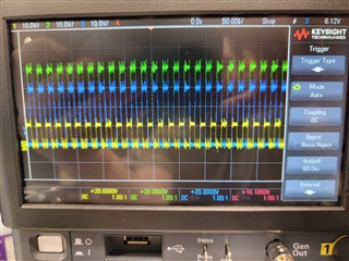
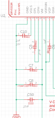
Using a DRV8353RS, I can spin a BLDC motor in FOC mode. This is a custom layout but, follows the recommended layout seen in the datasheet.

This is a dual supply setup so VM and Vdrain are not directly connected but, both are 15V

I have 3x boards that have failed in the same way where the DRV8353RS chip gets into a permanant failure mode.

Nothing appears wrong from the outside, I can communicate to the TI chip still, I can turn it on and off and at startup I have the following error codes on Register 0 and 1: 

0:0480

1: 0040

now, I can clear the register 0: 0400 error code but, the 0080 on reg0 and the 0040 on reg 1 remain no matter what.

The TI chip will then take an extra 110mA @15V on the VM supply and heat itself up to ~50C

This happens when VM and  Vdrain are connected to separate 15V (common grounds though). (Connecting to a common 15V also causes the same issue but it is immediate)

with the Vdrain pin floating and the Vm pin connected to 15V, I can still communicate as expected and the chip does not heat itself up or pull the extra 110mA.

So something is broken on the Gate driving side, I am just trying to understand what could be breaking internally or if the DRV8353RS locked itself into a mode that I can get it out of.

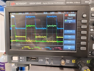
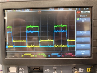
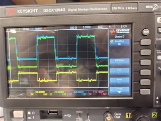
We are fairly early in our programming of the motor but can get a BLDC spinning in trapezoidal (not ideal) or FOC control schemes so I had assumed this was just due to our PWM not having the correct deadtime but, the DRV8353RS handles this by default.

this issue appears to happen when increasing voltage while the motor is spinning or, by increasing RPM while above 50V. 

  • Hi Michael,

    Could you measure the voltage of nFAULT, VDRAIN, VCP, and VGLS using an oscilloscope and provide me the wave form showing when nFAULT goes high?

    The errors from the registers are showing that there is an under voltage condition on these pins. 

    Thank you,

    Joshua

  • Nothing appears wrong from the outside, I can communicate to the TI chip still, I can turn it on and off and at startup I have the following error codes on Register 0 and 1: 

    Hi,

    Do you have high current on DRAIN supply that could mean damaged FETs? If not, then without VDRAIN supply, try to command the driver to spin the motor again while measure the GHX and GLX to see if the driver output are good or bad. If bad, then it has damaged output drive circuit. 

    Brian

  • I do not have a high current on Vdrain supply, when I turn on the Vdrain supply, the Vm supply goes high current ~110mA. 

    I still ran the test as you stated, without Vdrain supply connected, and tried to spin the motor.

    All GLx pins are 0V when trying to spin the motor

    All GHx pins are a 60Hz, 220mv pk-pk sine wave.


    I ran the test with Vdrain supply connected to 15V just to see the gates are up to.

    All GLx pins are 0V

    all GHx pins are ~13.5 or ~14V

    So the output drive circuit is damaged, obviously you cant tell me exactly what happened but, are there commons causes for this? I can try to replicate them on my end and I can can duplicate a failure, I can avoid the cause in the future.

  • Doing the test above: IN the images I have attached

    Channel 1 (yellow): Nfault

    Channel 2 (green): VGLS

    Channel 3 (blue): VCP

    Channel 4 (red): Vdrain

    Nfault goes high at turn on of Vdrain but, goes back to 0V

    Figure 1: With VM at 15V, Apply Vdrain as a separate 15V supply

    Figure 2: With Vdrain at 15V, Apply VM as a separate 15V supply

  • Hi Michael,

    Could you provide me the schematic of your system?

    Thank you,

    Joshua 

  • Private Message of schematic sent

  • The Nfault pullup is not shown but, it is installed 10k ohm

  • Hi Michael,

    I aligned with my team and some questions came up.

    1. Has this problem happened to every device or only some of them?

    2. At what point in operation does the device break, is it immediately, when trying to spin the motor, another point?

    3. Can you provide me the Idrive settings that are being used?

    4. Can you provide me an capture of VCP, GHx, SHx, nFAULT with a falling edge trigger on nFAULT?

    Thank you,

    Joshua

  • I ran the test with Vdrain supply connected to 15V just to see the gates are up to.

    All GLx pins are 0V

    all GHx pins are ~13.5 or ~14V

    GHx are DC at 14v and no switching?

    So the output drive circuit is damaged, obviously you cant tell me exactly what happened but, are there commons causes for this? I can try to replicate them on my end and I can can duplicate a failure, I can avoid the cause in the future.

    Yes, the driver has smart gate drive technology but if the FET t_rise and t_fall too long then this can cause overheat or shoot through, then the gate could have too high voltage which can damage the driver. Please use a good working board with Vdrain=30v to capture the waverform at GHx, GLx, SHx (motor phase voltag) for analysis. 

  • 1. Has this problem happened to every device or only some of them?

    This has happened to every board when I go outside of normal testing. (above 15V or above 700RPM)

    2. At what point in operation does the device break, is it immediately, when trying to spin the motor, another point?

    No matter the voltage, the board seems fine to startup until above 700RPM .

    No matter the voltage when the motor is spinning at 600+ RPM, And i change speeds to a lower RPM or a higher RPM the chip seems to break. (i think this is from a delay in the comms of our uController when I send the command, it kind of pauses, acting like a brake for a split second on the motor)

    3. Can you provide me the Idrive settings that are being used?

    Idrive is 1 A source, 2 A sink (on both high side and low side FETs) - this is both the max and the default value

    4. Can you provide me an capture of VCP, GHx, SHx, nFAULT with a falling edge trigger on nFAULT?

    Do you want to me to try and break the board as it has been breaking? and capture the moment it fails or just induce any type of fault I can?

  • GHx are DC at 14v and no switching?

    Yes, the GHx pins are just a flat DC of ~14V

    Please use a good working board with Vdrain=30v

    Should I keep Vdrain and Vm seperate for this test, so Vm= 15V and Vdrain = 30V?  or have Vm = Vdrain = 30V ?

  • I ran the test above using a good board spinning at 100RPM with Vdrain at 30V and Vm at 15V

    Channel 1: (yellow): GLA

    Channel 2: (Green): GHA

    Channel 3: (Blue): SHA

    I moved the signals' vertical positions in case there was anything that's more obvious when not on top of eachother. 

  • Hi Michael, 

    Joshua is currently out of office today but will aim to provide a response by the end of the week.

    Best,

    ~Alicia

  • I ran the test above using a good board spinning at 100RPM with Vdrain at 30V and Vm at 15V

    Channel 1: (yellow): GLA

    Channel 2: (Green): GHA

    Channel 3: (Blue): SHA

    I moved the signals' vertical positions in case there was anything that's more obvious when not on top of eachother.

    Hi Michael,

    I see almost zero deadtime between GLX and GHx; this can cause damage to FETs and driver. Please capture at 200ns/div, at GLx going low and going high so we can see the deadtime values.

    Brian

  • Re ran test zoomed in to 200ns/div

    Channel 1: (yellow): GLA

    Channel 2: (Green): GHA

    Channel 3: (Blue): SHA

    Channel 4: (red): PWM U-L

    To show both PWM signals we use have a 500ns Deadtime between them:

    Channel 1: (yellow): GLA

    Channel 2: (Green): GHA

    Channel 3: (Blue): PWM U-H

    Channel 4: (red): PWM U-L

  • To show both PWM signals we use have a 500ns Deadtime between them:

    Channel 1: (yellow): GLA

    Channel 2: (Green): GHA

    Channel 3: (Blue): PWM U-H

    Channel 4: (red): PWM U-L

    What are the PWM U-H and PWM U-L? Are they the pwm inputs to the driver corresponding to the output GHA and GLA? But then why U-H instead of A-H or A-L? If the 3 phase outputs are A, B, C, then the input should be A , B, C also, not U,V,W.

    Deadtime from GLA to GHA is about 400ns, and from GHA to  GLA is about 500ns, more than enough. What is the spec of the FETs?

  • sorry for the inconsistency in naming, yes PWM U-H and PWM U-L correspond to INHA and INLA on the DRV8353RS. This was to match our motor's UVW naming convention which is mirrored in the Net names and silkscreen.

    PWM U-H -> INHA

    PWM U-L -> INLA

    I am slightly concerned by the GLA going low and GHA going high, the GHA signal seems to have leakage, though it is still 0V Vgs and the Gate is not driven above that until the 500ns specified

    attached is datasheet for the FETs I am using: and an image of it's "timing" characteristics

    sidr870adp (2).pdf

  • Hi Michael,

    Based on the FET you are using, a 1A source and 2A Sink IDrive setting is a bit high, this is probably what is causing the voltage spikes in the GLA signal which could be damaging the VGLs linear regulator within the DRV8353.

    Please refer to this FAQ and this app note for how to choose the correct IDrive setting for you.

    Best Regards,

    Joshua

  • I am slightly concerned by the GLA going low and GHA going high, the GHA signal seems to have leakage, though it is still 0V Vgs and the Gate is not driven above that until the 500ns specified

    Both GHA and SHA going H right after GLA going L, instead of 500ns late. This is not leakage issue but because the SHA was driven by the other phases (SHB and SHC) and when SHA float higher then this also cause GHA to get higher for VGS=0v as you have expected. It's normal.

    The FET spec is a very good device. Gate rise and fall times are ok. At this point I really don't know what caused the problem but suggest to check Boot Cap as  too big cap can cause damage to boot charging current source;  check VM for high spike voltage.

    Brian

  • After a lot of testing, starting at 50mA source and 100mA sink and working our way up. The DRV8353RS no longer breaks until above 300mA source and 400mA sink

    The math for  the Vds rise and fall time still doesn't add up and is ~2x as fast as expected from the math where a 100mA Idrive should give us ~100nS fall of Vds we are actually seeing ~40ns to 55ns.

    We have noticed that when the breaking happens, it is during the initial startup of the motor. So unloaded we can startup at 50mA source, 100mA sink and then after startup change to a higher Idrive to reduce heat on the FETs. Is this changing of idrive while spinning a possible problem with the DRV8353RS?

    For now, lowering the idrive has seemed to fix the issue and we've had the motor spinning above 200W at 1000rpm. And the only way we can break the DRV8353RS anymore is by  changing the source above 300mA while spinning and under a load. Although, this has pushed us to adding some additional snubber circuits across all 6x Fets to reduce ringing and changing the FETs originally selected for ones with a lower gate charge to really make sue the DRV doesn't break again.

    The only additional question I have left on this:

    We have been trying to keep the "dirty" motor power separate from the power on the VM of the DRV8353RS and this is a dual supply application. This includes having grounds that are sperate on this board but connected after an external filter so they have the same reference. Do I need to have the grounds of the DRV8353RS connected as close as possible? I had sent the Sheet of the schematic that shows this "MTR GND" and just "GND" and it did't seem to raise any eyebrows before.

  • Jusr to confirm, is the boot cap the CPL-CPH cap? or VCP? CPL-CPH = 47nF and VCP = 1uF in this design.

  • The Fet gate charge pump cap is between VCP and VDrain which is charged to 11v. The other 47nF cap is charged to VDrain + 11V. (The circuit below with VM connected to the doubler upper FET seems to be a mistake, as it should be connected to the 11v source or 16v source, not VM as it is spec to 75v max and nobody want to drive the power FET gate at 75v!!!!). 

  • So, if the drawing in figure 29 is incorrect, I should be connecting the Vcp cap to VM not Vdrain?

    My configuration is a dual supply with VM ranging from 10V up to 30V and Vdrain ranging between 55V 85V.

    Below is my current configuration, where VM and Vdrain are sperate and Vcp is connected to Vdrain with a 1uF cap.

  • Hi Michael,

    Is this changing of idrive while spinning a possible problem with the DRV8353RS?

    I will have to look into this, I'll get back to you with a reply by Friday at the latest.

    Do I need to have the grounds of the DRV8353RS connected as close as possible?

    For split grounds we typically recommend having a low impedance and low inductive path connecting them on the PCB. For the low impedance and low inductive connection we recommend using a 0 ohm resistor.

    So, if the drawing in figure 29 is incorrect, I should be connecting the Vcp cap to VM not Vdrain?

    Your configuration is correct you should connect the Vcp cap to Vdrain.

    Despite VM being used internally, the charge pump controller will regulate the voltage on the CPL pin to ~10.5V, so long as VM > 15V, through switching the FETs accordingly. If VM < 15V, the CPL voltage and the average gate drive current will be lower.

    To see the effects lower VM voltage has on VCP please look at section 7.5 in the datasheet.

    Best Regards,

    Joshua

  • So, if the drawing in figure 29 is incorrect, I should be connecting the Vcp cap to VM not Vdrain?

    The 1uF bootstrap cap should be connected to VCP and VDrain (so to have VDrain + 11v for the upper FET gates), with the + polarity connected to VCP.

    What I said about the error in the Fig 29 is that the half-bridge upper FET Drain in the drawing should be connected to a 11v or 16v source and not VM as shown. If it's connected to VM then the power FETs will be driven at Vdrain + VM or the upper FET gate to source voltage will be 30v for VM=30, and this will blow up the FETs.

    Brian 

  • Hi Michael,

    Is this changing of idrive while spinning a possible problem with the DRV8353RS?

    Changing the idrive setting while the motor should not be a problem. See section 8.3.1.4.1 of the datasheet for more information:

    Best regards,

    Joshua