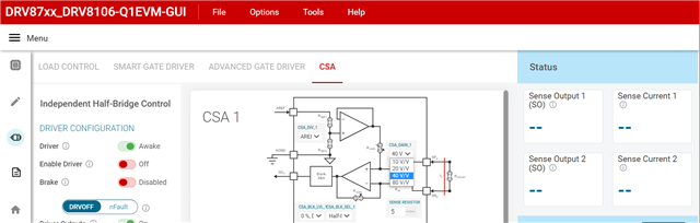
This thread has been locked.

If you have a related question, please click the "Ask a related question" button in the top right corner. The newly created question will be automatically linked to this question.

DRV8718-Q1: the parameter of Wide Common-Mode Current Shunt Amplifiers in DRV8718

Part Number: DRV8718-Q1

Hi team,

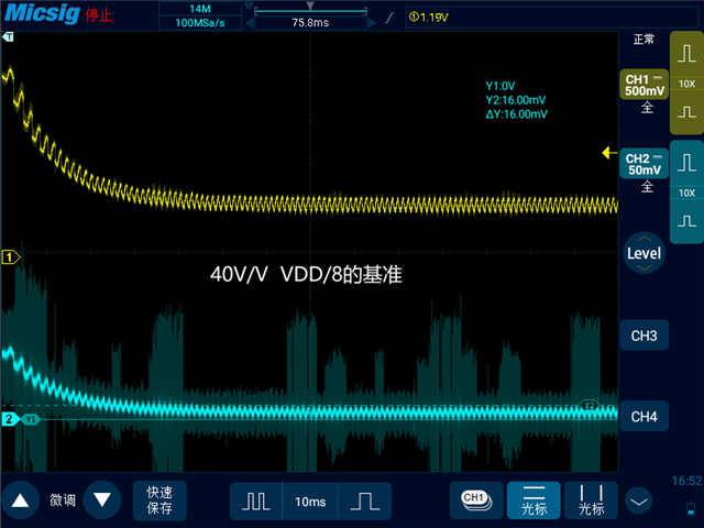
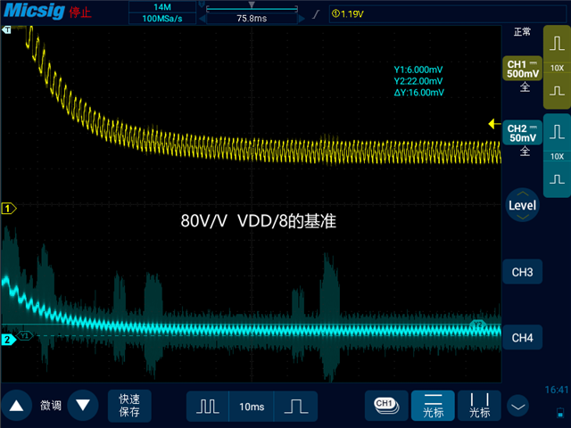
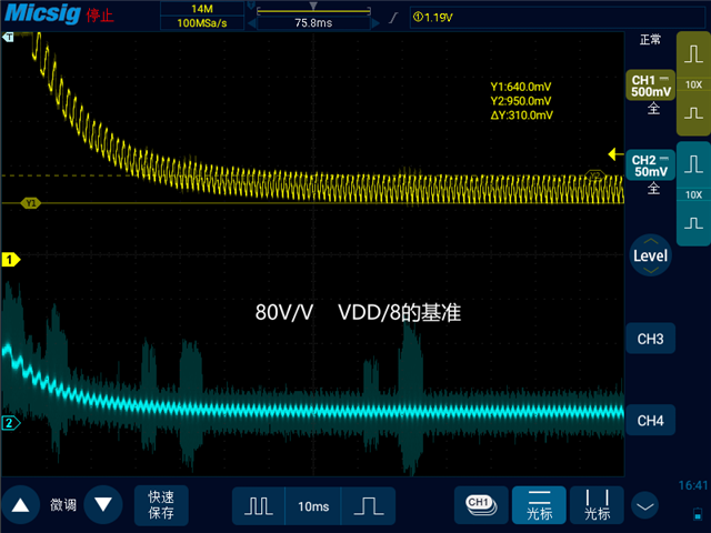
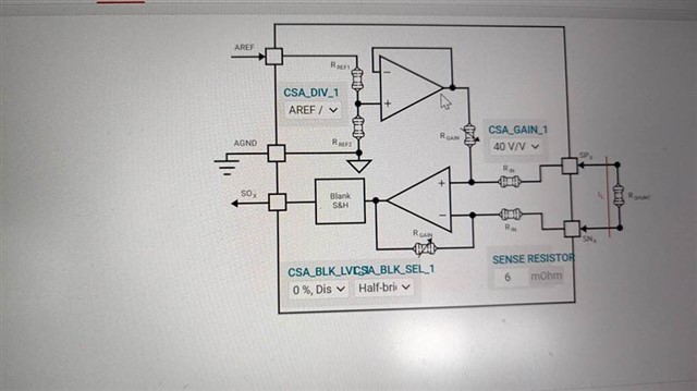
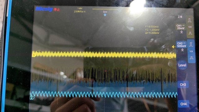
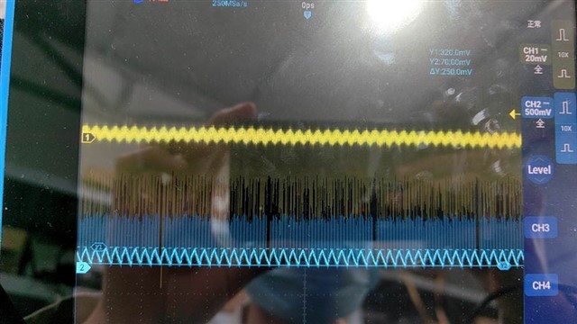
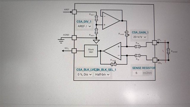
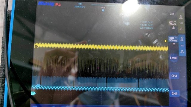
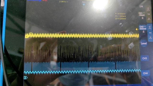
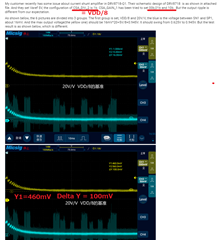
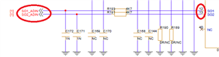
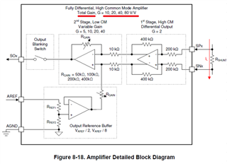
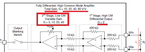
Could you please share the parameter of Wide Common-Mode Current Shunt Amplifiers in DRV8718? The spec in datasheet is partial. For example, the gain error is not stated in datasheet. And in addition to the datasheet, the customer want to know extra information about Current Shunt Amplifiers. Do we have more information can be provided? Or can we refer to the spec of other products?

  • Hale,

    Gain error is in there and a bunch of other specs.

    What else do you need?

    Regards,

    Ryan

  • Hi Ryan,

    Long time no contact and hope everything is well.

    My customer recently has some issue about current shunt amplifier in DRV8718-Q1. Their schematic design of DRV8718  is as shown in attached file. And they set Varef 5V, the configuration of CSA_DIV_2 is 1b. CSA_GAIN_1 has been tried to set 00b,01b and 10b.  But the output ripple is different from our expectation.

    As shown below, the 6 pictures are divided into 3 groups. The first group is set, VDD/8 and 20V/V, the blue is the voltage between SN1 and SP1, about 16mV. And the max output voltage(the yellow one) should be 16mV*20+5V/8=0.945V. It should swing from 0.625V to 0.945V. But the test result is as shown below, which is different.  


    The second group is set, VDD/8 and 40V/V, the blue is the voltage between SN1 and SP1, about 16mV. And the max output voltage(the yellow one) should be 16mV*40+5V/8=1.265V. It should swing from 0.625V to 1. 265V. But the test result is as shown below, which is different.    


    The third group is set, VDD/8 and 80V/V, the blue is the voltage between SN1 and SP1, about 16mV. And the max output voltage(the yellow one) should be 16mV*80+5V/8=1.905V. It should swing from 0.625V to 1.905V. But the test result is as shown below, which is different.    


    And we also tested the EVM, the test result is similar to the customer PCB test result.

    The first group is set 40V/V and Aref/8.

    The yellow is input voltage about 9.2mV; The blue is the output voltage, differential voltage should be 0.368V.The actual voltage is only 0.25V.

    The second group is set 20V/V and Aref/8.

    The yellow is input voltage about 9.2mV; The blue is the output voltage, differential voltage should be 0.184V.The actual voltage is only 0.14V.

    Now the customer has stopped PCB production. Could you help check if there is anything wrong in their configuration or in their PCB design? The schematic is attached in email.

  • Hale,

    Can you please post schematic?  Just section around sense amp showing sense resistor and where measurements were taken is ok.  No need to post whole schematic to protect IP.

    Regards,

    Ryan

  • Hi Ryan,

    I just sent the schematic via emial yesterday. You can check it.

  • Hi Hale,

    Based on given information, I believe DRV8718-Q1 works as expected.

    Basic formula is Vout =  (V_SPx - V_SNx ) * GAIN + REF

    1)  VDD/8 Offset. 

    On customer schematic, VDD=5V. Therefore REF = 5V/8 = 0.625V. Bellow waveform shows 460mV on the bottom. Let me judge this is similar/matching here. I guess customer is measuring on SO1_ADIN, not SO1 pin directly. It may cause some shift.

    2) GAIN, amplitude.

    Customer commented they change the GAIN 00b, 01b and 10b. Which means "Total GAIN" is 10,20,40.  

    Customer is showing waveforms as 20,40,80, but actually total gain is 10,20,40. Therefore waveform is matching to datasheet and fomula 

    Vout =  (V_SPx - V_SNx ) * GAIN + REF. 

    regards

    Shinya Morita

  • Hi Morita,

    Actually the total gain should be (10,20,40)*2=(20,40,80), as below.

    Also I test the EVB and the gain is 10~80. I think the total gain should be 20,40,80, not 10,20,40

  • Hi Hale san,

    Thank you for your question.

    2nd amp selection is 5,10,20,40. Then total gain is 10,20,40,80. Here is the description on datasheet  Fig 8-18.

    GUI also shows total gain 10,20,40,80.

    regards

    Shinya Morita

  • Yes, and the gain I mentioned in previous question is total gain,  20V/V to 80V/V.

    I don't understand what you mean, as below. The total gain is 20V/V, 20V/V, 80V/V. How is the waveform matching to the datasheet and fomula?

  • Thank you for your question. Here is why.

    " CSA_GAIN_1 has been tried to set 00b,01b and 10b." This is information for customer settings.

    Then 00b,01b,10b are GAIN 10,20,40 as follows.

    regards

    Shinya Morita

  • Morita,

    Sorry for the misunderstanding. The gain set should be 01,10,11. And actually you can check their test on EVB, the gain is also not meet their expectation. 

  • Hi Morita,

    I think that the customer test method has something wrong. The op-amp gain should be ok. Thanks for your patience. I will check the test method again with customer.

    Another question:

    If we use resistor to divide the output voltage of SOx, will the output drive capacity 

    be reduced? The customer want to use ADC of MCU to sample SOx voltage. But the voltage of SOx exceed the range. They want to use resistor about 100 to divide voltage. Do we have any advice or experience?

  • Hi Hale,

    Thanks you for the update. Could you create new post for additional question? Then let me close this post.

    regards

    Shinya Morita