This thread has been locked.

If you have a related question, please click the "Ask a related question" button in the top right corner. The newly created question will be automatically linked to this question.

DRV8908-Q1EVM: Issues communicating with MSPM0 as SPI Controller

Part Number: DRV8908-Q1EVM
Other Parts Discussed in Thread: DRV8908-Q1, , LP-MSPM0G3507

Hi Team,

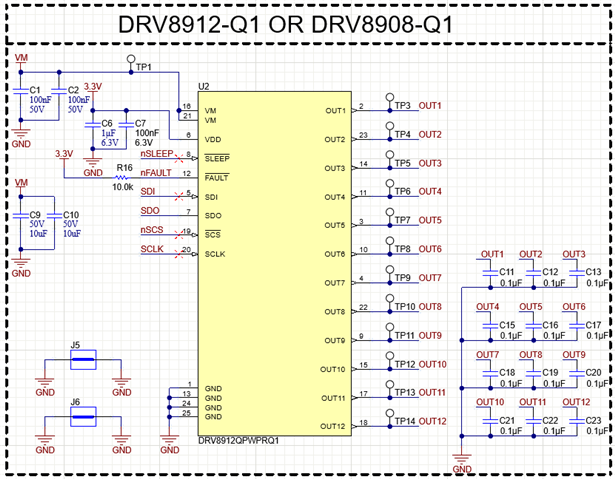
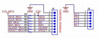
I'm working on building up a SPI driver for communicating with this EVM, however am running into issues & struggling to debug. I have taken a stock EVM, and depopulated resistors R10, R11, R12, and R13 shown below to separate the DRV8908-Q1 from the on-board MCU.

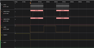
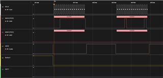
I then perform two SPI writes to the device, one which disables open load diagnostics for all the channels, and one which should set the HB1_HS_EN bit high. See below for a Saleae plot showing the transaction. Unfortunately I am not seeing the OUT1 signal come high as I would expect based on this transaction.

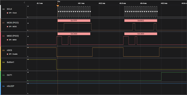
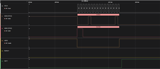
When I use an unmodified, Stock EVM with the GUI, once again taking care to disable the OLD diagnostics, I see the below transaction for triggering HB1_HS_EN. As you can see, this does in fact make OUT1 high as expected.

Can someone help me understand where I might be going wrong, and why I'm not seeing a response on the MISO line for my MSPM0 driver?

Thanks!

- Andy

  • Andy,

    Looking at nSCS in your plot, I see a narrow pulse before going LOW.  If you look at figure 1 in the datasheet, there is a t(HI_nSCS) spec which is the minimum HIGH time before going low.  See table 7-6.  Is this being violated in your communication?

    Regards,

    Ryan

  • Hi Ryan,

    Good catch, the original plot was violating the tHI_nSCS spec (was 80ns high time vs. required 600ns). I've corrected this, but still am not seeing any response from the device. See below for Saleae plot. Let me know if you have any other questions about the set-up, I've just connected ground & all SPI lines between the LP-MSPM0G3507 and the DRV8908-Q1EVM  and applied 12V to the VBAT rail.

    Regards,

    Andy

  • Andy,

    Do you have 3.3V or 5V on the VDD pin?  This is the logic supply to the device.  This powers SDO output as SDO output is a push-pull.  The supply should match your MCU supply.  

    Regards,

    Ryan

  • Hi Ryan,

    VDD is directly tied to 3.3V on the DRV8908EVM (See below snippet from design files):

    I've also confirmed my SPI peripheral is also 3.3V (see below capture of SCLK showing both digital & analog trace captures):

    Regards,

    Andy

  • Hi Ryan,

    I figured out the issue. Stereotypical debug mishap... I had removed the R14 resistor (nSLEEP) in between my first test where I was violating the tHI_nSCS and the second test where this violation was fixed. Removing it caused the nSLEEP pin to be floating which translated to the device being asleep. Sweat smile

    Here's a working Saleae log:

    Regards,

    Andy