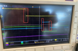
Ch1:cs
Ch2:clk
Ch3:miso,no data
Ch4:mosi
The operation corresponding to the waveform is read Configuration Register(0x07), The data sent by MCU is 0x4747
nSLEEP is tested as high level and VDD is 3.3v
This thread has been locked.
If you have a related question, please click the "Ask a related question" button in the top right corner. The newly created question will be automatically linked to this question.
Ch1:cs
Ch2:clk
Ch3:miso,no data
Ch4:mosi
The operation corresponding to the waveform is read Configuration Register(0x07), The data sent by MCU is 0x4747
nSLEEP is tested as high level and VDD is 3.3v
Hi Ryan,
Thanks for your reply.
This is the relevant schematic diagram,The communication pins of SPI are directly connected to the MCU terminal.
We tested two devices, and the results were the same. Do you see anything wrong with the schematic?