Hi,
I am having trouble with simulating the DRV8244-Q1 H variant.
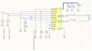
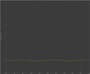
I have made a simple schematic that you can see below. The problem is that there is almost nothing on the output.
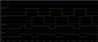
The NFAULT pin goes HIGH after sending the correct startup sequence on the NSLEEP pin (30us LOW, so that means that it clears faults and doesn't go to sleep).
Also the MODE pin is directly connected to GND which means it is operating in the PH/EN mode.
If someone can check the schematic and give any input it would be appreciated.
Below is the differential voltage between OUT1 and OUT2 from the simulation:
Regards,
Marin