This thread has been locked.

If you have a related question, please click the "Ask a related question" button in the top right corner. The newly created question will be automatically linked to this question.

DRV8323: [SOLVED] SPI Variant, Overtemperature warning on VDS register

Part Number: DRV8323

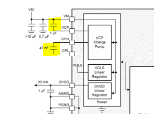
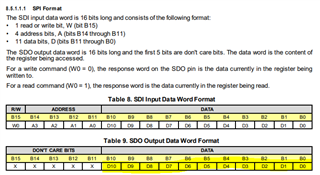
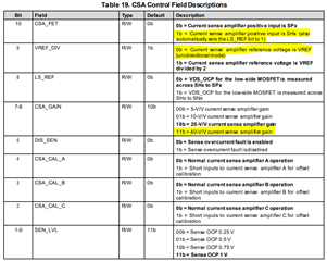
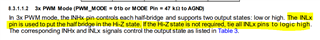
We are building a new driver and we are testing our firmware, after reading status of registers we can to notice that fault register 1 is all clear but fault register 2 is 511 decimal value. There is also over temperature warning even though motor is not connected / drive is not even given any signal, The physical temperature of the IC seems less than 40-50 degree maybe even less.

What can be the reason for this fault? since we are testing the current given to overall drive is limited to 500mA and total current drawn along with MCU is hardly 60mA max.

Kindly suggest what needs to be checked to clear all the warnings

  • Hi Amrith,

    Thank you for posting to the Motor Driver's forum!

    Based on what is being reported by fault register 2, it looks like the following are being reported:

    • overcurrent on phase C sense amplifier
    • OTW
    • charge pump undervoltage
    • gate drive faults on both the HS and LS of all MOSFETs

    What is your IDRIVE set to? It could be the case that your IDRIVE setting is too large. Also what are the capacitors that you are using for the charge pump?

    Best,

    ~Alicia

  • Hi Alicia,

    Thank you for responding.

    I have used 1uF capacitor X5R 50V (part number CL10A105KB8NNNC) for Bulk capacitor , only change from the above values is that the 10UF between Vm and GND is not used but a 4.7uF is used which I am planning to replace .

    OTW is getting reported even though the driver isnt even warm , not hardly warm compared to room temperature

    I am using a 5mOhm current sense resistor with 40V/V setting on all but only on pase C the current sense warning appears

    Yes The IDRIVE values are default and seems to be high enough , let me try to reduce these and try as per the example application calculations.

    PS: I was able to test a motor , but it wasnt able to start on its own , I had to manually rotate it to start after which it works . I was testing it with very small motor hardly 70mA total current is drawn along with MCU power. Once I am confident I am planning to test with 15A motors

  • Hi Amrith,

    Yes The IDRIVE values are default and seems to be high enough , let me try to reduce these and try as per the example application calculations.

    Depending on what the Qgd of the MOSFETs that you are using is, the default IDRIVE settings of this device could be causing the device to be slewing the GHx and GLx too fast. 

    I will need to look into what could be causing the OTW to trigger and will aim to provide an update by the end of this week.

    Best,

    ~Alicia

  • Thank You Alicia

    These are the values after writing the SPI registers

    ADR_FAULT_STAT = 0
    ADR_VGS_STAT = 511
    ADR_DRV_CTRL = 120
    ADR_GATE_DRV_HS = 1023
    ADR_GATE_DRV_LS = 0
    ADR_OCP_CTRL = 896

    Will provide an update with IDRIVE and TDRIVE value calculated . Hopefully that will clear a lot of faults,

    One thing you can notice is GATE_DRV_LS register is zero even after writing some values , I am currently testing 1x PWM to test hardware and later on we will be switching to 3xPWM . Can You please tell me why GATE DRIVE LS is zero even after writing  some values (11 bit , even defalut value is non zero)? 

  • looks like my SPI read/write is not proper :( .

  • Hi Amrith,

    ADR_FAULT_STAT = 0
    ADR_VGS_STAT = 511
    ADR_DRV_CTRL = 120
    ADR_GATE_DRV_HS = 1023
    ADR_GATE_DRV_LS = 0
    ADR_OCP_CTRL = 896

    To clarify, these are decimal values, correct?

    looks like my SPI read/write is not proper

    Could you please describe what is going on in more detail (is the SPI register not being correctly accessed, etc.), this will help to narrow down where the issue could be occurring? Are you able to share waveforms (from a logic analyzer) of the SPI reads and writes that you are doing?

    Best,

    ~Alicia

  • Hi Alicia,

    Sorry Alicia , I forgot to update the SPI mode , realised it was SPI mode 1 not SPI mode 0

    these are the default vales (only two registers are not matching the datasheet)

    yes all values are decimal

    ADR_DRV_CTRL = 0 (matching the default)

    ADR_GATE_DRV_HS = 1023 (matching default)

    ADR_GATE_DRV_LS = 2047 (matching default)

    ADR_OCP_CTRL = 345 (matching defaults)

    ADR_CSA_CTRL = 3267 ----> not matching the default value (643) !

    ADR_CSA_CTRL = 3267  ----> not matching the default value !

    only this register is now having a different value after strartup , can you please suggest why this might be happening?

    Also one more question before doing any SPI transaction the signals semms to be noisy but after doing a read or write , the signals are no longer showing any noise

  • Hi Amrith,

    ADR_CSA_CTRL = 3267 ----> not matching the default value (643) !

    Converting 3267 to binary you would get (1100 1100 0011)2 which is a total of 12 data bits which I am curious as to what the MSB would be as there should only be 11 data bits, as specified below:

    Aside from that, ignoring the MSB which would give us (100 1100 0011)2 or 1219 in decimal, it appears that the highlighted bits below are different from the default:

    From what was mentioned previously,

    I am using a 5mOhm current sense resistor with 40V/V setting

    Would it be possible that you are writing to this register which may be the reason why it is not at the default value?

    Best,

    ~Alicia

  • Hi Alicia,

    Thank you for checking the values.

    The values and SPI communication issues seems to be resolved. We did face some issue because of SDO line needs a pull up resistor but that was resolved inititially. The soldering of our board also seems to be questionable.

    I have gone through 1x PWM , 3X PWM and 6X PWM control

    For 3x PWM the commutation table shows INLx and INHx as inputs meaning all 6 PWM / GPIO inputs are required for 3X PWM. This seems to be the case even for 6X PWM. However the description says INHx is used to control both high side and low side mosfets .

    Kindly clarify this for me

    Thank You,

    Amrith

  • Hi Amrith,

    Regarding the commutation tables, what is shown are possible GHx/GLx/SHx outputs given some INLx/INHx inputs. In the case of 3x PWM mode, INLx is used to put the half-bridge into the Hi-Z state. Should the Hi-Z state not be needed, then you can tie INLx to logic high.

    Unlike 6x PWM mode which does use all six inputs to control the states of GHx/GLx, for 3x PWM mode INHx is what determines whether or not GLx is high, and GHx is low, or GHx is high, and GLx is low. This is confirmed by the truth table for 3x PWM, as we can see that INLx only determines whether both GLx and GHx is pulled low and SHx is in the Hi-Z state. Whether or not GHx/GLx is pulled high depends only on whether or not INHx is high or low, as for both instances, INLx are high. 

    Best,

    ~Alicia

  • Thank you very much Alicia for your support. We were able to do a 6 step commutation !

    Closing this thread . Thank once again!

  • Hi Amrith,

    Glad I was able to help!

    Best,

    ~Alicia