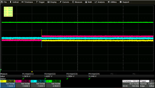
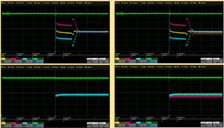
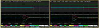
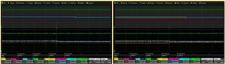
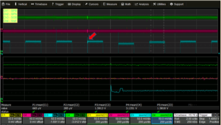
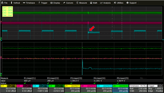
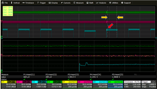
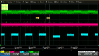
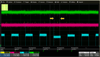
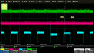
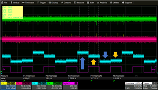
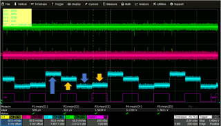
We're seeing a similar issue with phase B using DRV8353*. What was the resolution to this issue?

-
Ask a related question
What is a related question?A related question is a question created from another question. When the related question is created, it will be automatically linked to the original question.