


In this E2E FAQ we will cover frequently asked questions about MCx devices in schematic and layout stages of design.
1. How should I configure the Thermal Vias on the BLDC motor driver device?
A common equation we use for the thermal resistance of vias is noted here:

where,
- Length is thickness of PCB board
- Area is (number of vias x pi x (R^2−(R−t)^2)) , where R is radius of vias and t is plating thickness
- Thermal conductivity is that of copper: 0.385 W/mm-K
Some conclusions to make from this:
- The higher the number of vias, lesser the thermal resistance.
- Plan to add as many vias as possible in thermal pad for better heat dissipation. Datasheet layout is only a suggestion – add as many vias as allowed by PCB manufacturer.
- It may be better to add more smaller vias than a few larger vias – optimize based on above formula and PCB manufacturer rules
2. How should I configure the GNDs. Do I need a PGND and an AGND?
Use different ground planes (whenever possible) for AGND and PGND to isolate the switching noise from low-voltage signals (referenced to AGND).
Tie PGND and AGND through a 0-ohm resistor; 0-ohm can be replaced with suitable inductor/ferrite bead to isolate high frequency noise while tying the two ground planes for DC signals.
DGND can be tied to AGND plane and GND_BK can be tied to PGND plane.

3. Do I need to connect all three VM and PGND pins to VM and PGND respectively?
Use all three VM and PGND for connecting to respective VM and PGND power Cu planes/pours.
Not using all VM/PGND pins for connections will increase the RDS_ON by approximately 10-15mΩ per pin compared to datasheet values.

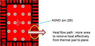
4. Should I leave NC pins floating or connect them to GND?
While not required, engineers often connect the NC pins 22-25 to AGND. These pins (circled in yellow below) can be connected to thermal pad and to AGND plane for better heat dissipation:

5. How should I configure the Buck Regulator external components?
If there is no/light external load (< 20mA) on buck converter it is recommended to do the following:
- Set BUCK_CL to 150mA
- Use LBK = 22µH
- Saturation current rating of:
- If inductor is too big, it can be replaced with RBK = 22Ω. RBK should be sized to handle the dissipation
If there is an external load (> 20mA) on buck converter it is recommended to do the following:
- Set BUCK_CL to 600mA
- Use LBK = 47µH
Saturation current rating of:
6. When not using the DACOUT pins, should I leave them floating or connect them to GND?
When not using the DACOUT pins, it is best to leave them floating.
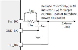
7. Do I need to populate the buck external components if I am not using the buck regulator?
With the exception of the MCT831xZ devices which must have the external buck components populated, buck converter external components can be avoided and device can be powered up by connecting AVDD to FB_BK (as seen below):

When doing this, leave SW_BK floating, GND_BK tied to PGND/AGND, and tie FB_BK to AVDD.
Some other things to note if you are looking to implement this into your system. When you do this, you may experience additional power loss due to AVDD powering FB_BK which could lead to worse thermal performance/derating. This is the reason it is not an official datasheet recommendation. The second caveat is that engineers must disable the buck by writing 1b to BUCK_DIS. The buck will be switching and giving a buck UV fault which won't stop the motor operation, but can become a nuisance.
This may help you save BOM costs for buck converter passive components but will cause additional power losses. For example, (VM-AVDD) * 20mA in MCx8316.
