


Hi team,
1) The hardware circuitry is basically the same as the specification recommendation, except that VM power is 15 V and VDRAIN power is 24 V, when the driver is charged with the VDS overcurrent protection after power up. The H-bridge outputs a triangle wave at the top and a PWM wave at the bottom (OCP is now set to the maximum threshold).
When VM is changed to 24V, complementary PWM is output on both the G-stage of the upper and lower tubes, waveform is good and VDS overcurrent protection is not reported. Why? (Voltage meets specification, charge pump voltage is normal)
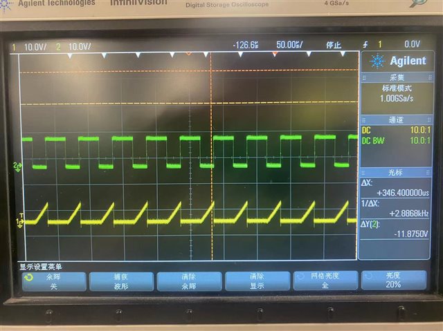
(Yellow is the G-class abnormal waveform of the upper tube and green is the G-class waveform of the lower tube)
2) SA_OC, SB_OC, SC_OC overcurrent is reported when firmware is written to the CSA control register. An overcurrent error is reported even if the default configuration is written. However, adding a 1-ms delay before writing to the register eliminates overcurrent issues. Are there also logic or timing requirements for register writes?
Could you help check this case? Thanks.
Best Regards,
Cherry
