


Hi team,
1) What are the differences between coast and brake (fast current decay versus slow decay) and the pros and cons?
coast (00) fast current decay
brake(11)Brake; low-side slow decay
2) Normal operating current is 120mA, hardware stall current Itrip 800mA, measured effective value is 330mA, software overcurrent 270mA. Is it reasonable?
3) The electrolytic capacitor on VM is 47uF, what is its purpose? Is it ok to remove it?
4) When current exceeds Itrip, hardware protection is triggered, how does the corresponding OUT1,OUT2 change? The 00 mode is being used.
5) Below is the measured waveforms, could you help review is there any issues?
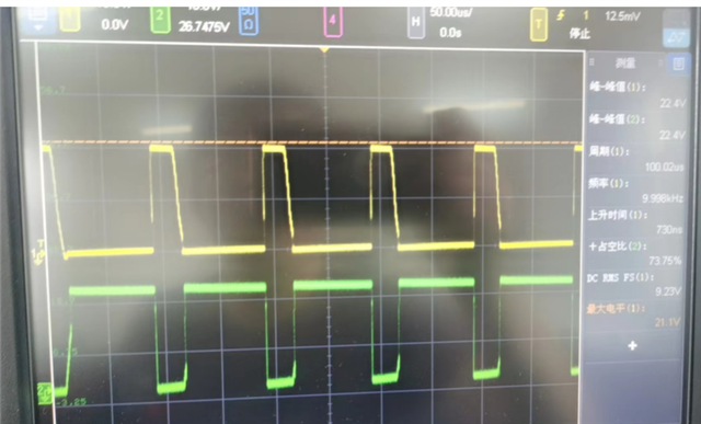
At normal operation
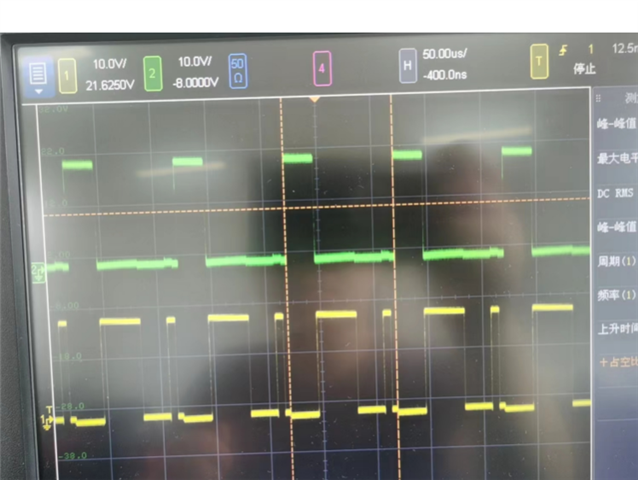
At stall
Could you help check this case? Thanks.
Best Regards,
Cherry
