This thread has been locked.

If you have a related question, please click the "Ask a related question" button in the top right corner. The newly created question will be automatically linked to this question.

DRV8305: There is a thermal noise issue in the motor drive

Part Number: DRV8305

Hi team,

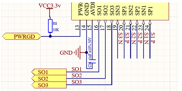
Motor drive scheme: Stm32f401+dvr8305, dvr8305 peripheral circuit is built according to 8.2 typical application of datasheet. Vcc=3.3V, PVDD=12v (operating from adjustable power supply).

The dvr8305 is driven using the stm32 monolithic chip, using the motor drive strategy of St Corporation. Previously there was a problem at startup, the motor would stop at the start of the open loop phase, the nfault pin would go low, customer guess it was due to PVDD undervoltage. This issue is resolved after modifying PVDD_UV_PWRGD (0xB bit2). The PVDD undervoltage is still present at start-up and the motor can operate in the initial open loop phase but will stop when closed loop is reached. 

So the customer designed a 6-step control program to drive the motor start-stop. The motor is found to be slow and hot. Here are the oscilloscope measurements: (The oscilloscope has only 2 channels, only 2 waveforms can be displayed, so only information about motor a is measured) 

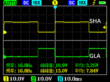
DRV8305-phase A input pin signal 

DRV8305-Phase A Output Pin (Motor not connected) 

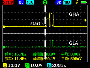
DRV8305-Phase A output pins and some zoomed-in view (connecting motor) 

DRV8305-Phase A Voltage Measurement (Channel 1) with Motor connected 

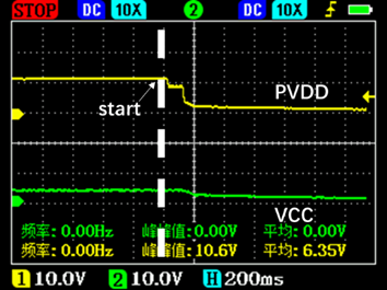
DRV8305-operating voltage PVDD (was 12v, but buck to 4.3V) and Vcc (connected to motor) 

It seems like the measured waveform is not the same as the normal waveform, could you help check this case? Thanks.

Best Regards,

Cherry

  • Hi Cherry,

    Thank you for the question! I believe one change the customer should make is to use a buck that has an output between 4.4V and 45V (4.3V is a little low, see the attached image). The DRV 8305 has an internal LDO to handle voltages like these. This may be a commutation issue. That said, I'll get back to you with a better answer tomorrow.

    Best,

    Eli

  • Hi Eli,

    Thank you for the support.

    They are using an adjustable regulated power supply of 12v and drv8305 is forced down to 4.3V when it's operating.

    Thanks and regards,

    Cherry

  • Hi Cherry,

    Thank you for the clarification. The device is specified to operate within the recommended ratings in the datasheet and that recommended operation is between 4.4V and 45V. The current voltage being used is below the recommended operating conditions. It can operate lower (as low as 4.3V) with the LDO but this will not drive the motor or yield good performance. Please let me know if operating at a higher voltage does not solve the issue.

    Best,

    Eli

  • Hi Eli,

    The 12V adjustable power supply is provided above and the driver board drops to 4.3V during operation, which is not the normal operating range. The motor drive board was originally powered from a 12V (error 1V) battery and converted to 3.3V by an LDO chip. 

    The following details are based on the 12v battery powered, six-step control method:

    With the motor unconnected, the voltage at which the drive board is operating is shown in the figure below.

    It can be seen that the outputs of GHA, GLA, and SHA are good.

    When the motor is connected, the drive board stops working for no more than 0.3 s, the outputs of GHA, GLA, and SHA are shown below:

    PVDD = 12v, Vcc = 3.3V before the driver board is not working.

    However, the failure occurs and stops in less than 0.2 s after the start of operation, and PVDD and Vcc have changed, as shown in the figure below:

    The entire drive board does not work and the voltage at PVDD and VCC are as follows: 

    Thanks and regards,

    Cherry

  • Hi Cherry, 

    Today is a US holiday, so many of our team members are out of office currently, returning later this week - please anticipate a delayed response 

    Best Regards, 
    Andrew 

  • Hi Cherry,

    Is the fault still listed as PVDD_UV or is it different? Also, what is the customer's slew rate?

    Best,

    Eli

  • Hi Eli,

    Is the fault still listed as PVDD_UV or is it different?

    The DRV8305 register information returned by the driver board is shown below.

    1 after power up

    2 Initialization

    3six step control

    4 Fault condition 

    5 after fault

    0x1:   0

    0x2:   0

    0x3:   0

    0x4:   0

    0x5: 344

    0x6: 344

    0x7: 216

    0x8:   0

    0x9:  20

    0xa:   0

    0xb: 10a

    0xc: 2c8

    0x1:   0

    0x2:   0

    0x3:   0

    0x4:   0

    0x5: 344

    0x6: 344

    0x7: 216

    0x8:   0

    0x9: 2a1

    0xa:   0

    0xb: 10e

    0xc: 2c8

    0x1:   0

    0x2:   0

    0x3:   0

    0x4:   0

    0x5: 344

    0x6: 344

    0x7: 216

    0x8:   0

    0x9: 2a1

    0xa:   0

    0xb: 10e

    0xc: 2c8

    0x1: 490

    0x2:   0

    0x3:  20

    0x4:   0

    0x5: 344

    0x6: 344

    0x7: 216

    0x8:   0

    0x9: 2a1

    0xa:   0

    0xb: 10e

    0xc: 2c8

    0x1:   0

    0x2:   0

    0x3:   0

    0x4:   0

    0x5:   0

    0x6:   0

    0x7:   0

    0x8:   0

    0x9:   0

    0xa:   0

    0xb:   0

    0xc:   0

    Register 16 is represented as b10-b0, for example 0b 100 1000 0001 is represented as 481 and 0b 000 0000 0001 is represented as 1. The drive flow of the driver board operates on the drv8305 as follows: Power up → Initialization → six step control.

    It can be seen that PVDD_UVFL and VCPH_UVFL report errors for a short period of time when the fault occurred, after which the entire register information is always 0. 

    Also, what is the customer's slew rate?

    Mosfet being used is IRFH7085PbF, MOSFET QGD=36NC is specified in datasheet.

    MOSFET Slew Rate1 = 36 nC (QGD) / 60 mA (IDRIVEN) = 600 ns

    MOSFET Slew Rate2 = 36 nC (QGD) / 50 mA (IDRIVEP) = 720ns

    Thanks and regards,

    Cherry

  • Hi Cherry,

    The device is also reporting a AVDD under voltage fault. Can the customer check to ensure they are following the schematic recommendations listed on page 16 of the datasheet? The E2E post (+) DRV8353: Charge Pump undervoltage Fault - Motor drivers forum - Motor drivers - TI E2E support forums may provide some insight on their issue. Ensuring that capacitors are properly rated for the voltage may be a factor when dealing with charge pump errors. Generally, we like to use ceramic capacitors that are rated at twice the voltage they will be experiencing.

    Best,

    Eli

  • Hi Eli,

    The following figure shows the information about the components surrounding the drv8305 chip in the design driver board schematic. VBat_D = PVDD = 12v, VCC3.3V = Vcc = 3.3V in the figure. C22 and C23 are rated for 50V nominal and should be fully adequate. Is there anything that can be improved? 

    Thanks and regards,

    Cherry

  • Hi Cherry,

    Thank you for the schematic.

    PVDD_UVFL and VCPH_UVFL report errors for a short period of time when the fault occurred

    The cause of this issue will be C18 and C19.  They are rated for 16V when they are connected to VBat_D which will cause DC biasing. Due to this the effective capacitance of the capacitors will decrease, VCPH has an ABS_MAX rating of PVDD+12V so let's use a voltage rating for C18 and C19 that is double this (~50V). Please let me know if this solves your problem.

    Best,

    Eli

  • Hi Eli,

    The customer tested with 2.2uf/50V and 4.7uf/50V capacitors, but the problem still persists:

    Thanks and regards,

    Cherry

  • Hi Cherry,

    I'll align with the team and get back to you on this by Friday.

    Best,

    Eli

  • Hi Cherry,

    Thank you for your patience. Can the customer give VCPH to GHx and VCP_LSD to GLx resistance measurements? Can they also send over waveforms of the charge pump relative to GND? Have they tried connecting their motor to an EVM and seeing if the issue persists when it is not their board being used? Can they measure AVDD when the issue occurs?

    Best,

    Eli

  • Hi Eli,

    After the customer has wired the evaluation board of the DRV8305 to the base board of the STM32, the test results are as follows: 


    DRV8305-EVM

    custom board

    RVCPH-GHA(Ω)

    0.439

    1.720M

    RVCPLSD_GLA(Ω)

    0.486

    0.495M

    VVCPH-GNDV

    22v(No motor connected )9.6v(motor connected )

    22v(No motor connected )unkown(motor connected )

    VAVDD-GNDV

    4.5v

    4.51v(0V at fault)

    The DRV8305-EVM also has a 090 fault alert in the 0x01 register during operation, similar to the driver board. However, the six-step control method works properly in other driving solution. The following is the six-step driver method, g_iMotorPFlag is set to 1 every 10ms: 
    //dead loop
    
    if(g_iMotorPFlag)
    
    {
    
     g_iMotorPFlag=0;
    
    count1++;
    
    liubukongzhi(count1);
    
    if(count1>=6) count1=0;
    
    }
    
     //Six-step control method 
    
    void liubukongzhi(int j)
    
    {
    
        switch(j)
    
        {
    
            case 1:
    
                HAL_GPIO_WritePin(INH_A_GPIO_Port,INH_A_Pin,GPIO_PIN_SET);//A+
    
                HAL_GPIO_WritePin(INL_A_GPIO_Port,INL_A_Pin,GPIO_PIN_RESET);    
    
                HAL_GPIO_WritePin(INH_B_GPIO_Port,INH_B_Pin,GPIO_PIN_RESET);
    
                HAL_GPIO_WritePin(INL_B_GPIO_Port,INL_B_Pin,GPIO_PIN_SET);//B-  
    
                HAL_GPIO_WritePin(INH_C_GPIO_Port,INH_C_Pin,GPIO_PIN_RESET);
    
                HAL_GPIO_WritePin(INL_C_GPIO_Port,INL_C_Pin,GPIO_PIN_RESET);
    
                break;
    
            case 2:                
    
                HAL_GPIO_WritePin(INH_A_GPIO_Port,INH_A_Pin,GPIO_PIN_SET);//A+
    
                HAL_GPIO_WritePin(INL_A_GPIO_Port,INL_A_Pin,GPIO_PIN_RESET);    
    
                HAL_GPIO_WritePin(INH_B_GPIO_Port,INH_B_Pin,GPIO_PIN_RESET);
    
                HAL_GPIO_WritePin(INL_B_GPIO_Port,INL_B_Pin,GPIO_PIN_RESET);    
    
                HAL_GPIO_WritePin(INH_C_GPIO_Port,INH_C_Pin,GPIO_PIN_RESET);
    
                HAL_GPIO_WritePin(INL_C_GPIO_Port,INL_C_Pin,GPIO_PIN_SET); //C-
    
                break;
    
            case 3:                
    
                HAL_GPIO_WritePin(INH_A_GPIO_Port,INH_A_Pin,GPIO_PIN_RESET);
    
                HAL_GPIO_WritePin(INL_A_GPIO_Port,INL_A_Pin,GPIO_PIN_RESET);    
    
                HAL_GPIO_WritePin(INH_B_GPIO_Port,INH_B_Pin,GPIO_PIN_SET);//B+
    
                HAL_GPIO_WritePin(INL_B_GPIO_Port,INL_B_Pin,GPIO_PIN_RESET);    
    
                HAL_GPIO_WritePin(INH_C_GPIO_Port,INH_C_Pin,GPIO_PIN_RESET);
    
                HAL_GPIO_WritePin(INL_C_GPIO_Port,INL_C_Pin,GPIO_PIN_SET);//C-
    
                break;
    
            case 4:                
    
                HAL_GPIO_WritePin(INH_A_GPIO_Port,INH_A_Pin,GPIO_PIN_RESET);
    
                HAL_GPIO_WritePin(INL_A_GPIO_Port,INL_A_Pin,GPIO_PIN_SET);//A-
    
                HAL_GPIO_WritePin(INH_B_GPIO_Port,INH_B_Pin,GPIO_PIN_SET);//B+
    
                HAL_GPIO_WritePin(INL_B_GPIO_Port,INL_B_Pin,GPIO_PIN_RESET);    
    
                HAL_GPIO_WritePin(INH_C_GPIO_Port,INH_C_Pin,GPIO_PIN_RESET);
    
                HAL_GPIO_WritePin(INL_C_GPIO_Port,INL_C_Pin,GPIO_PIN_RESET);
    
                break;
    
            case 5:                
    
                HAL_GPIO_WritePin(INH_A_GPIO_Port,INH_A_Pin,GPIO_PIN_RESET);
    
                HAL_GPIO_WritePin(INL_A_GPIO_Port,INL_A_Pin,GPIO_PIN_SET);//A-
    
                HAL_GPIO_WritePin(INH_B_GPIO_Port,INH_B_Pin,GPIO_PIN_RESET);
    
                HAL_GPIO_WritePin(INL_B_GPIO_Port,INL_B_Pin,GPIO_PIN_RESET);    
    
                HAL_GPIO_WritePin(INH_C_GPIO_Port,INH_C_Pin,GPIO_PIN_SET);//C+
    
                HAL_GPIO_WritePin(INL_C_GPIO_Port,INL_C_Pin,GPIO_PIN_RESET);
    
                break;
    
            case 6:                
    
                HAL_GPIO_WritePin(INH_A_GPIO_Port,INH_A_Pin,GPIO_PIN_RESET);
    
                HAL_GPIO_WritePin(INL_A_GPIO_Port,INL_A_Pin,GPIO_PIN_RESET);    
    
                HAL_GPIO_WritePin(INH_B_GPIO_Port,INH_B_Pin,GPIO_PIN_RESET);
    
                HAL_GPIO_WritePin(INL_B_GPIO_Port,INL_B_Pin,GPIO_PIN_SET);//B-
    
                HAL_GPIO_WritePin(INH_C_GPIO_Port,INH_C_Pin,GPIO_PIN_SET);//C+
    
                HAL_GPIO_WritePin(INL_C_GPIO_Port,INL_C_Pin,GPIO_PIN_RESET);
    
            break;
    
        }
    
    }
    
     
    Thanks and regards,
    Cherry
  • Hi Cherry,

    Thank you for the response. I'll align with my team and get back to you by Tuesday. In the meantime, would you be able to ask the customer if they could provide the following?

    - Waveforms of the charge pump relative to GND

    - More details regarding your power supply. Can the customer switch out their power supply and try a new one and give us waveforms of the performance? This seems to be the main issue as the faults are all PVDD_UV, CP_UV and AVDD_UV errors and the capacitor ratings seem to be good.

    Thank you for your patience.

    Best,

    Eli

  • Hi Eli,

    - More details regarding your power supply.

    The power supply is one MD-3010D adjustable power supply and the other is a 12-V battery. 

    model number

    operating voltage

    operating current

    output power

    MS3010D

    0.00V-32.0V

    0.00A-10.2A

    300W

    Customers are currently testing with the DRV8305-EVM evaluation board and using the six-step driving method to drive the DRV8305-EVM evaluation board, the output voltage of the adjustable power setting (i.e. PVDD) is 12V. The adjustable power supply shows that the output voltage drops to 7.3 V and the output current is 9.4 A during the six-step drive method. VVCPH-GND and VPVDD-GND are measured by the oscilloscope to be 12.4 V and 5.27 V, respectively. Battery power stops working for a short period of time after start-up and cannot be measured.

    The adjustable power supply works properly when driving the same motor in other motor drive schemes, so they assume it's not a problem with the power supply. 

    BTW, the customer is wondering if TI's MCU and motor drive scheme are required to use the DRV8305? Can the DRV8305 be compatible with other external motor drive schemes? Like odrive, simplefoc, stmc, and so on? 

    Thanks and regards,

    Cherry

  • Hi Cherry,

    Thank you for the reply. I'll align with my team and get back to you on Wednesday.

    Best,

    Eli

  • Hi Cherry,

    Thank you for waiting. What is the current limit set on their supply? When a load is connected to the supply (i.e. the motor) and there is a current limit set on the output, the voltage will change accordingly. This is likely the issue the customer is facing. Also, DRV8305 is compatible with other MCUs. 

    Best,

    Eli