This thread has been locked.

If you have a related question, please click the "Ask a related question" button in the top right corner. The newly created question will be automatically linked to this question.

DRV8323: Problem when enable gate driver DRV8323 from sleep mode

Part Number: DRV8323

Hi,

I have a problem when enable gate driver DRV8323 from sleep mode,

I write ENABLE pin to low to go to sleep mode, after that I write pin ENABLE to high but it not work, all output power to Motor are 24V and motor can not run (I use power 24V).

can you tell me how to wake up DRV8323 form sleep mode.

Thank you.

  • Hi Long, 

    For the wake-up condition to be met VM must be greater than the internal undervoltage lockout condition voltage of at least 5.4 V when ENABLE is being written high for a wake-time of 1ms. Can you measure and provide the waveform of the voltage on VM and ENABLE, as well as the state of nFAULT when writing the ENABLE pin high? 

    You may be able to do an ENABLE reset pulse by applying a "high-to-low-to-high transition" on the ENABLE pin where the low period of the sequence should fall with the tRST time block window.

    Hope this information helps lead to a solution.

    Best Regards,

    -Joshua

  • Dear Joshua,

    Thanks for your support. The issue with wake up the gate driver is ok.

    But today I suddenly detect a problem about my hardware PCB.

    My desgin uses IC DRV 8323RH so with GAIN input pin and VDS pin we have a mistake with designs:

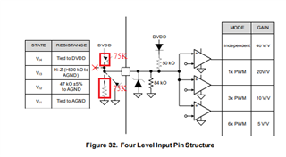
    With GAIN input pin we inserted 2 res 75K to VDD and 75K to GND line picture below:

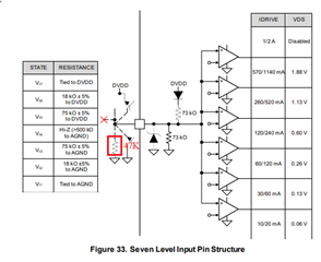
    With VDS input pin we inserted res 47K to GND

    I know it's wrong, It don not follow with datasheet , I am wrong with swapping design for 2 pin (It should be Hz state for Vds pin for VDS threshold = 0.06 (2 res 75K to VDD and GND)  and 47K to GND for GAIN pin (Gain = 10V/V) ). But now we can not change the hardware PCB, because it is closed in sealed box, we can open it.

    So we can not change the  hardware PCB with true design,

    I know the ic use comparator between V input voltage pin with a threshold, with our wrong design,

    V GAIN input = 1.88 V

    V DS input = 0.9V

    with the wrong design the gain of IC = ? and VDS threshold  = ? And have any risk with wrong design?

    Brs,

    Longpt

  • Hi again Long, 

    Happy to hear your wake-up issue had a solution. 

    I don't recommend operating the device outside of its intended specs/circuit design characteristics. I will have to look into the possible effects on gain and VDS threshold with your unique configuration. 

    Best Regards,

    -Joshua

  • Yes Joshua,

    Please let me know the value of GAIN and VDS overcurrent trip voltage with my wrong configuration as soon as posible.

    I see that my wrong configuration. It feel like the GAIN = 20V/V (Because I have to double Iq ref for Iq loop in FOC controller to get the desired torque), and VDS overcurrent trip voltage it can be 0.13V or 0.26 V?

    Brs

    Longpt

  • another information , the board is stll working normally.

  • Thanks for the additional info, Long.

    Still looking into those possible effects/cautions.

    Thank you for your patience,

    -Joshua

  • Joshua
    We need the confirmation to make a decision that fix or not fix the board. Because it is quite difficult to fix the board, like i said before the board is closed in a sealed box, if we try to open it, It may cause the other risk for product. 
    So if there is no serious effect/caution with it, We will not fix the board.
     
    Brs,
  • Hi Long, 

    After deliberation I can't guarantee the performance of the device gain outside of the intended and tested pin-setting spec range. 

    Regarding the VDS Threshold, it may float from 0.13- x -0.26, and you will have to test on your device manually to determine the exact value.  Attempting to open the part should be out of the question for the reason regarding other potential damage. 

    My best recommendation for ideal and intended performance would have to be to redesign your PCB with the correct configuration in mind.

    If not possible, I would continue testing your input/outputs of the device to ensure that no affected parameter breaches the ABS-MAX.   

    Best Regards,

    -Joshua

  • Joshua,

    Thanks for reply.

    What about the Gain, Is it equal to 20, I have tested and found that the gain is 20. I tested and got that V gain input > 1.726V, the GAIN is 20. With my design the V gain input = 1.88V so it is 20. But I wonder if there is any case that the gain may float from 10 - 20 like you said with VDS threshold , if the gain value may float, It is a big issue with me, If is constant 20, That would be ok.

    With VDS threshold If may float from 0.13 to 0.26V and only effect to the protection current threshold of the board ( = VDS threshold / RDS_mosfet) and as long as it does not affect other components of IC, I think that would be ok.

    Please confirm me the gain in this case is constant 20 or not?

    Brs,

  • My drive use mosfet FDMS86350 with Rds_on = 2.1mohm, with the VDS Threshold, it may float from 0.13- x -0.26 , the current threshold from 61A to 123 A, and My applycation never to reach this level, I think the only risk here is If there is any caution with drive , this protection level current will never protect the driver and motor.  Is that right?

  • Hi Long,

    The gain is harder to determine where it may float if it does at all due to the unusual configuration. I am not sure how sensitive the pin may be during device operation outside of the known 20V/V gain you are seeing, and do not believe it will be easy to give a recommendation. 

    Regarding the VDS threshold, you are correct that it will only be tripped from either 61-123A which could be much higher than it may ever experience depending on your application. How much nominal current do you plan for? The VDS threshold is able to go down to 0.06V, but once again that would require a design change. 

  • How much nominal current do you plan for?

    --> My application has nominal current 3A.

    The VDS threshold is able to go down to 0.06V, but once again that would require a design change. 

    --> Yes, Design change is a must for new batch of products.  But with the integrated product I decide I will not fix the board, because it is still working normally, currently during the phase test we do not detect any problem with the driver.

    The gain is harder to determine where it may float if it does at all due to the unusual configuration. I am not sure how sensitive the pin may be during device operation outside of the known 20V/V gain you are seeing, and do not believe it will be easy to give a recommendation. 

    With this concern, Can you collaborate with higher expert motor driver DRV8323 to give me recommentation?

    Brs,

  • Hi Long, 

    The previous response I gave regarding the unknown nature of the unique gain pin configuration was with extra guidance, and the recommendation was to not use the configuration at all due to such possible unknown volatility (which you won't be in further instances, as you said).  More test and validation with the exact unique configuration would be required to make an additional judgement. 

    Best Regards,

    -Joshua