I am working on a FOC ESC and using DRV8353HRTAT (40 pin QFN). After going through the data sheet i have made the schematic according to what i have understood. But i still doubt if i have interpreted the information correctly.
My interpretations -
IDRIVE (Pin 28) - Idrive > Qgd / tr which for the mosfets i have choosen is - 21nC/10ns = 2.1 amps. So this pin should be supplied with 2.1 amps.
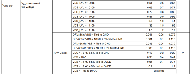
VDS (Pin 29) - trip current point - Vds > Imax * Rds(on) which for my case is - 100A * 4.4mOHM = 0.44 volts. So this pin should be given 4.4 volts.
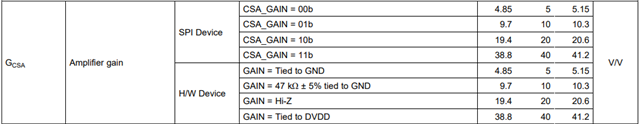
Gain (Pin 30) - gain settings - for my case - as vref is 3.3V, Rsense = 1.6mOHM, Imax is 100 amps, gain should be more than 20/20 v. So im going with a gain of 20/20.
It would be of great help if my assumptions are verified.
DRV schematic image 
Entire schematic picture