This thread has been locked.

If you have a related question, please click the "Ask a related question" button in the top right corner. The newly created question will be automatically linked to this question.

DRV8844: Motor drivers forum

Part Number: DRV8844
Other Parts Discussed in Thread: DRV8220, DRV8935

Hi,

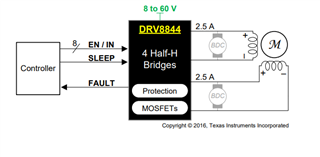
I am using DRV8844 to drive 2 valves right now and it works as expected. 

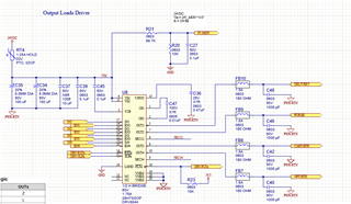
I am planning to add 2 additional heaters, schematic as below. 

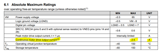
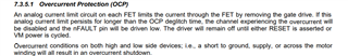
As I understand the datasheet each pin OUT1..4 can support 2.5A also the VM is directly connected to the mosfet internally to the IC. So the VM is getting redirected to the fets. 

The valves on out 1 and out 2 consume around 400mA together

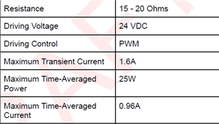
The heaters on out 3 and out 4 will consume around 1.5A.

All these outputs will be on at the same time. I wanted to know if the IC itself can handle all the pins with high current at the same time. 

For example Vm = 24V and Combined current of OUT1..4 = 10A

If so apart from adding in wider traces is there anything else which needs to be considered like hear dissipation etc? 

Schematic

Heater specs

Thank you,

Bhavya

  • Hey Bhavya,

    The DRV8844 can supply up to 2.5-A peak or 1.75-A RMS output current per channel (with proper PCB heatsinking at 24 V and 25°C) per H-bridge.  However, it can't do this simultaneously - 2.5A is also the peak current output for the device, with an absolute max of 3A.  

    I have ran the thermal calculation for your system using the DRV8220 Power Dissipation and Output Current Capability section because it goes into far more detail than the DRV8844 datasheet.  The same specifications from the DRV8844 can be applied to the DRV8220 formulas.  

    Your system total current = (0.4A + 0.4A + 1.5A + 1.5A) = 3.8A

    Pvm = Vvm * Ivm = 24V * 0.001A = 0.024W

    Psw = 24V * 3.8A * 90nS * 20 kHz = 0.164W (rise and fall time are 30ns to 150ns, so an average of 90nS)

    Prds = IRMS^2 * (RdsonHS + RdsonLS) = 3.8A^2 *  (0.25Ω x 1.5 + 0.25Ω x 1.5) = 10.83 W

    Tj= (Ptot x RθJA) + Ta = (0.024W + 0.164W + 10.83W) * 31.6 °C/W + 25 °C = 373°C  

    So unfortunately the DRV8844 device will hit overtemperature of 160°C if it was driving this load.  

    The recently released DRV8962 would work for your application, as it can drive a peak simultaneous current of 10 amps. 

    Regards,

    Jacob

  • Hi Jacob,

    I may be wrong but I guess Bhavya would like to use four channels independently, all four loads connected to separate outputs and GND. Then Rds losses would be much lower. Currents would be conducted just by one half-bridge mosfet at a time. Then Rds losses would be:

    Prds = 2 x (1.5^2 x 0.25Ω x 1.5)  +  2 x (0.2^2 x 0.25Ω x 1.5) = 1.69 + 0.03 = 1.72W

    Power losses of around 2W would not be so bad to deal with lets say 4 or 6 layer board. Of course, proper PCB design would be needed to dissipate those 2 watts.

    Regards,

    Grzegorz

  • Hi Grzegorz,

    Yes my plan is to use the 4 channels independently to drive separate loads but all the loads will be turned on at the same time. 

    So in that regards what Jason pointed out takes a stand. By what I understand is total current Out1+Out2+Out3+Out4 < 2.5A

    However, it can't do this simultaneously - 2.5A is also the peak current output for the device, with an absolute max of 3A.

    Now I'm more confused as the datasheets shows below image and does not mention if it simultaneous or not.

    If I read under OCP section it mentions each FET is limited to 3A

  • Hi Bhavya,

    I think the limit is 1.75A rms or 2.5A peak per channel, then if you keep channel turned on constantly its max current would be 1.75A. For PWM wave you would get 2.5A peak limit and 1.75A rms limit per channel.  I guess theoretical limit of whole DRV8844 is the sum of all channel limits but Rds losses would be rather impossible to dissipate. I think your main problem will be to dissipate 2W of heat. I would start with PCB design similar to DRV8935 EVM board, 4- layers, lots of thermal vias under the chip and around, 2-3 GND planes to spread the heat.

    You can consider also using DRV8935, it has a bit lower Rdson of Mosfets and its HTSSOP version is available on TI website.

    https://www.ti.com/tool/DRV8935PEVM

    Regards,

    Grzegorz

  • Hey Grzegorz and Bhavya, 

    Ahh you are correct, after talking with coworkers I confirmed it is 2.5A limit per FET not total.  Grzegorz is correct, I concur with his most recent answer above. The 2.5A limit per channel definitely applies, and the OCP that will trigger between 3A and 5A.  

    Regards,

    Jacob

  • Hi Grzegorz and Jacob,

    Thank you very much for clarification. I know how to move forward with the design. 

    Thank you,

    Bhavya