This thread has been locked.

If you have a related question, please click the "Ask a related question" button in the top right corner. The newly created question will be automatically linked to this question.

DRV8353: 6X PWM, 3X PWM, 1x PWM

Part Number: DRV8353

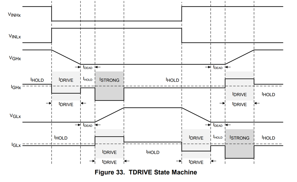
Hi, using the 6x PWM mode, we are observing dead times between high side and low side switching that seem to completely ignore the Tdrive and Tdead settings.  Can you help me understand why this is the case?  I get the impression that in 6x mode, the VINHx and VINLx determine the state of the gate drives directly, and that only the Idrive setting is meaningful - this is what our traces suggest.  However the datasheet for the chip is not clear to us on this subject.

Does the 3X PWM mode behave differently?  The timing diagrams we found in the datasheet for our exact chip (DRV8353) suggest yes.  The low side gate's state being determined by the VINHx input + Tdrive + Tdead makes sense.  

Your help gaining clarity would be much appreciated.

-S

  • Hey Shemuel,

    By ignoring Tdrive and Tdead timing do you mean that it is taking longer or shorter duration? I would like a little it more clarification on what is being observed (expected vs observed).

    Also please consult this post on Tdrive as it contains an updated tdrive diagram compared to the DS.

    https://e2e.ti.com/support/motor-drivers-group/motor-drivers/f/motor-drivers-forum/1162578/drv8323-clarification-of-tdrive-state-machine/4457975#4457975

    In 3X PWM the INHx pin controls each half-bridge and supports two output states: low or high. Please consult section 8.3.1.1.2 for more info.

    Best,
    Akshay

  • Read through the other thread.  It answers a lot of questions (really wish it was in the datasheet).  Thank you.

    What would be most helpful is more elucidation on the way the chip behaves in different PWM modes, and for different tdrives.  For example,

    1) in 6x PWM, does the only difference in operation lie in the truth table?  There is another string that suggests in 6x mode, the PWM inputs to the DRV directly control gate states.  What is correct?   (https://e2e.ti.com/support/motor-drivers-group/motor-drivers/f/motor-drivers-forum/637861/drv8323-various-pwm-modes )

    2) if tdrive is too short to cover both high and low gate transitions + deadtime, what happens?

    3) if tdrive is longer than the time needed to cover both high and low gate transitions + deadtime, what happens?

    4) For 2 & 3 above, do the answers change, depending on PWM mode?

    5) How does TMS dead band impact the timing of the signals?  Are their timing entirely determined by the 2V threshold and DRV deadband or does a TMS-sourced dead band impact DRV timing (for 6x, 3x, 1x)?

    Thanks,

    -S

  • Hey Shemuel,

     We have noted the changes needed to the DS and are working on DS updates internally.

    1) The PWM mode changes are stated in the truth table. The PWM inputs in 6x mode are related to the gate signals  with some propagation delay.

    2) If the Tdrive is too small and the correct gate voltage threshold has not been reached by the end of tdrive then you get a gate drive fault.

    3) If the Tdrive is longer than needed then there is less chance of issues. Its just that the Idrive current will be applied for longer. And the VGLS will not be checked for longer so if there is a gate to source short then Idrive will be applied for a a little longer through the short,

    4) The general concepts are the same across the PWM modes.

    5) What is TMS dead band? The gate drive faults are determined by the high side and low side gate voltage thresholds in relation the Tdirve and Idrive (DS section (8.3.6.5)

    Best,

    Akshay

  • Hi Akshay,

    The TMS deadband is the deadband generated by the Texas Instruments TMS320F2879D we also incorporated in our system.  We understand its effect is to create a delay between the high and low side command inputs for a given phase.  The timing diagram shows the high and low command inputs arriving simultaneously.  We assume the effect of the TMS deadband is to cause a relative delay in the arrival of these two signals at the DRV.  Is this correct?  

    In general, what is the effect of TMS deadband on the operation and state table transitions of the DRV?

    -S

  • Hey Shemnuel, 

    So the TMS device is adding a software dead time correct? Then the effect would be that the INH and INL will now have the time added between them which would couple into when the GH and GL voltages change.

    The voltage thresholds are checked at the end of tdrive for GDF.

    Best,

    Akshay

  • Hi Ashkay, sorry for the long absence.  I understood that each time the INH and INL change, it causes a change in the state table of the DRV 8353 as it operates in 6X PWM mode.  This change in the state stable caused by the later arrival of the INL signal will truncate the just-initiated Tdrive interval and start a new one based on the new INH/INL state.  Is this not correct?  

    In general, I'm looking for a detailed understanding of what causes the DRV to switch the FETs.  Is it the Vgs detection mechanism described in the DRV module + DRV-specified dead time?  If yes, what is the precise logic that determines how a later arrival of an INL signal will be incorporated into the timing of idrive application to the high side and low side FETs?

  • Hey Shemuel,

    The first component of the TDRIVE state machine is automatic dead-time insertion. Dead time is period of time between the switching of the external high-side and low-side MOSFETs to make sure that they do not cross conduct and cause shoot-through. The DRV835x family of devices use VGS voltage monitors to measure the MOSFET gate-to-source voltage and determine the correct time to switch instead of relying on a fixed time value. This feature allows the gate-driver dead time to adjust for variation in the system such a temperature drift and variation in the MOSFET parameters. An additional digital dead time (tDEAD) can be inserted and is adjustable through the registers on SPI devices.

    I am a little confused on the last question. Would you be able to elaborate a little more?

    If yes, what is the precise logic that determines how a later arrival of an INL signal will be incorporated into the timing of idrive application to the high side and low side FETs?

    Is this the section in the DS your question is referring to?

    "The second component focuses on parasitic dV/dt gate turnon prevention. To implement this, the TDRIVE state machine enables a strong pulldown ISTRONG current on the opposite MOSFET gate whenever a MOSFET is switching. The strong pulldown last for the TDRIVE duration. This feature helps remove parasitic charge that couples into the MOSFET gate when the half-bridge switch-node voltage slews rapidly."

    Best,
    Akshay

  • The answer is definitely not in the data sheet.  If INL is delayed to INH by 3 uS, for example, but tdrive is set to 2000 nS - what happens?  What is the comprehensive logic including Vgs sense, Tdead from the DRV, dead time inserted via the INH / INL signals, and tdrive that determines when the gates will be driven?

    As an example, take a look at this scope capturen that's attached.  Tdead from the DRV is set to 400 nS.  Yet, I'm getting 0 dead time and very likely some shoot through - how is that happening?  Only the detailed logic in the DRV will inform on this question.

    KEY
    Yellow is Phase A high side gate

    Pink is Phase A low side gate

    Green is Phase B high side Gate

    Blue is Phase A phase voltage

    White is Phase A Vgs

    -S

  • Hey Shemuel,

    I will look more into it and provide feedback next week.

    Best,
    Akshay

  • Hey Shemuel,

    If INL is delayed to INH by 3 uS, for example, but tdrive is set to 2000 nS - what happens?

    There is a separate Tdrive for high side and low side. So the INH timer would be expired by the time the INL timer starts. And from then on if the gate voltage does not meet the threshold then it triggers the fault as expected.

    As for the waveform, i think that the 400nS deadtime is being implemented. 

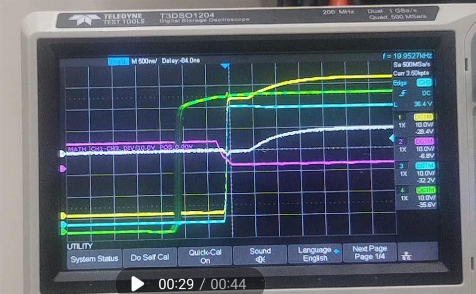
     The hs waits 400ns before turning on,
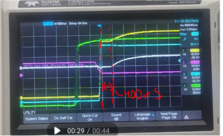
    Best,
    Akshay

  • Hey Shemuel,

    Marking the thread as closed for now. If your question was addressed please mark the thread as resolved.

    Please let us know if you have more questions or if you have new questions please post them as a new thread.

    Best,
    Akshay