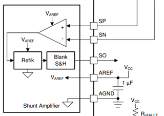
I am considering a circuit with the configuration in Figure 7-11. Please answer the following questions.
・Where is the power supply for each amplifier located?
(Example: 1st = VCP / 2nd, Reference Buffer = DVDD)
・When PVDD < VPVDD_UV, Current Sense = Disabled (Table 7-9). What happens to the SO output voltage when disabled?