This thread has been locked.

If you have a related question, please click the "Ask a related question" button in the top right corner. The newly created question will be automatically linked to this question.

DRV8329AEVM: Developing new board

Part Number: DRV8329AEVM
Other Parts Discussed in Thread: DRV8329, CSD19506KTT, UCC27284, , C2000WARE

Hi Team,

The half-bridge gate driver replaces the DRV8329+CSD19506KTT with 3 UCC27284 to control the BLDC and there're 2 issues may need your help:

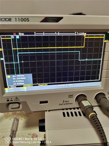
1) Configure PWM in hal.c, EPWM3 has no waveforms, while the other two phases have PWM waves:

// GPIO227->EPWM3A->M1_UH
GPIO_setPinConfig(GPIO_227_EPWM3_A);
GPIO_setDirectionMode(227, GPIO_DIR_MODE_OUT);
GPIO_setPadConfig(227, GPIO_PIN_TYPE_STD);

// GPIO230->EPWM3B->M1_UL
GPIO_setPinConfig(GPIO_230_EPWM3_B);
GPIO_setDirectionMode(230, GPIO_DIR_MODE_OUT);
GPIO_setPadConfig(230, GPIO_PIN_TYPE_STD);

// GPIO0->EPWM1A->M1_VH
GPIO_setPinConfig(GPIO_0_EPWM1_A);
GPIO_setDirectionMode(0, GPIO_DIR_MODE_OUT);
GPIO_setPadConfig(0, GPIO_PIN_TYPE_STD);

// GPIO1->EPWM1B->M1_VL
GPIO_setPinConfig(GPIO_1_EPWM1_B);
GPIO_setDirectionMode(1, GPIO_DIR_MODE_OUT);
GPIO_setPadConfig(1, GPIO_PIN_TYPE_STD);


// GPIO2->EPWM2_A->M1_WH
GPIO_setPinConfig(GPIO_2_EPWM2_A);
GPIO_setDirectionMode(2, GPIO_DIR_MODE_OUT);
GPIO_setPadConfig(2, GPIO_PIN_TYPE_STD);

// GPIO3->EPWM2_B->M1_WL
GPIO_setPinConfig(GPIO_3_EPWM2_B);
GPIO_setDirectionMode(3, GPIO_DIR_MODE_OUT);
GPIO_setPadConfig(3, GPIO_PIN_TYPE_STD);

2) Refer to DRV8329AEVM control flow for UCC27284 with non-SPI interface. Could you help share how to port the software and is there any reference documentation available? The software is based on the C2000\C2000Ware_MotorControl_SDK_4_02_01_00\solutions\universal_motorcontrol_lab\f280013x project.

Could you help check this case? Thanks.

Best Regards,

Cherry

  • Hey Cherry,

    I will take a look at this and provide feedback next week.

    Best,
    Akshay

  • Hey Cherry,

    It seems that the question more pertains to C2000Ware so I will let them comment.

    Best,
    Akshay

  • Hi Akshay,

    Thanks for the support from you and C2000 team and expect your update.

    Thanks and regards,

    Cherry

  • Hello,

    Apologies for the delayed response.

    First, what C2000 device are you using- is it the F280013x?

    Second, is there any difference in the ePWM configuration code utilized for ePWM3 vs ePWM1 and 2? If this is based on the universal motor control lab, also please check if ePWM6 is being used instead of ePWM3- this is the case for a few different C2000/inverter device combinations.

    Third, if you're looking to port Universal Motor Control Lab code, there's a section in the UMCL User's Guide which discusses porting to other C2000 MCUs and inverter boards. What else are you looking for?

    Regards,
    Jason Osborn

  • Hi Jason Osborn,

    Thank you for the response.

    There are currently three sets of PWM waveforms, but the dead-band configuration in the PWM wave is not working. The PWM wave uses ePWM1, ePWM2, and ePWM3. The code also confirms that DB is configured, please see the codes below: 

    void HAL_setupPWMs(HAL_MTR_Handle handle)
    {
    
    HAL_MTR_Obj *obj = (HAL_MTR_Obj *)handle;
    uint16_t cnt;
    
    uint16_t pwmPeriodCycles = (uint16_t)(USER_M1_PWM_TBPRD_NUM);
    uint16_t numPWMTicksPerISRTick = USER_M1_NUM_PWM_TICKS_PER_ISR_TICK;
    
    // disable the ePWM module time base clock sync signal
    // to synchronize all of the PWMs
    SysCtl_disablePeripheral(SYSCTL_PERIPH_CLK_TBCLKSYNC);
    
    // turns off the outputs of the EPWM peripherals which will put the power
    // switches into a high impedance state.
    EPWM_forceTripZoneEvent(obj->pwmHandle[0], EPWM_TZ_FORCE_EVENT_OST);
    EPWM_forceTripZoneEvent(obj->pwmHandle[1], EPWM_TZ_FORCE_EVENT_OST);
    EPWM_forceTripZoneEvent(obj->pwmHandle[2], EPWM_TZ_FORCE_EVENT_OST);
    
    for(cnt=0; cnt<3; cnt++)
    {
    // setup the Time-Base Control Register (TBCTL)
    EPWM_setTimeBaseCounterMode(obj->pwmHandle[cnt],
    EPWM_COUNTER_MODE_UP_DOWN);
    
    EPWM_disablePhaseShiftLoad(obj->pwmHandle[cnt]);
    
    EPWM_setPeriodLoadMode(obj->pwmHandle[cnt], EPWM_PERIOD_DIRECT_LOAD);
    
    EPWM_enableSyncOutPulseSource(obj->pwmHandle[cnt],
    EPWM_SYNC_OUT_PULSE_ON_SOFTWARE);
    
    EPWM_setClockPrescaler(obj->pwmHandle[cnt], EPWM_CLOCK_DIVIDER_1,
    EPWM_HSCLOCK_DIVIDER_1);
    
    EPWM_setCountModeAfterSync(obj->pwmHandle[cnt],
    EPWM_COUNT_MODE_UP_AFTER_SYNC);
    
    EPWM_setEmulationMode(obj->pwmHandle[cnt], EPWM_EMULATION_FREE_RUN);
    
    // setup the Timer-Based Phase Register (TBPHS)
    EPWM_setPhaseShift(obj->pwmHandle[cnt], 0);
    
    // setup the Time-Base Counter Register (TBCTR)
    EPWM_setTimeBaseCounter(obj->pwmHandle[cnt], 0);
    
    // setup the Time-Base Period Register (TBPRD)
    // set to zero initially
    EPWM_setTimeBasePeriod(obj->pwmHandle[cnt], 0);
    
    // setup the Counter-Compare Control Register (CMPCTL)
    EPWM_setCounterCompareShadowLoadMode(obj->pwmHandle[cnt],
    EPWM_COUNTER_COMPARE_A,
    EPWM_COMP_LOAD_ON_CNTR_ZERO);
    
    EPWM_setCounterCompareShadowLoadMode(obj->pwmHandle[cnt],
    EPWM_COUNTER_COMPARE_B,
    EPWM_COMP_LOAD_ON_CNTR_ZERO);
    
    EPWM_setCounterCompareShadowLoadMode(obj->pwmHandle[cnt],
    EPWM_COUNTER_COMPARE_C,
    EPWM_COMP_LOAD_ON_CNTR_ZERO);
    
    EPWM_setCounterCompareShadowLoadMode(obj->pwmHandle[cnt],
    EPWM_COUNTER_COMPARE_D,
    EPWM_COMP_LOAD_ON_CNTR_ZERO);
    
    // setup the Action-Qualifier Output A Register (AQCTLA)
    EPWM_setActionQualifierAction(obj->pwmHandle[cnt],
    EPWM_AQ_OUTPUT_A,
    EPWM_AQ_OUTPUT_HIGH,
    EPWM_AQ_OUTPUT_ON_TIMEBASE_UP_CMPA);
    
    EPWM_setActionQualifierAction(obj->pwmHandle[cnt],
    EPWM_AQ_OUTPUT_A,
    EPWM_AQ_OUTPUT_LOW,
    EPWM_AQ_OUTPUT_ON_TIMEBASE_DOWN_CMPB);
    
    EPWM_setActionQualifierAction(obj->pwmHandle[cnt],
    EPWM_AQ_OUTPUT_A,
    EPWM_AQ_OUTPUT_LOW,
    EPWM_AQ_OUTPUT_ON_TIMEBASE_ZERO);
    
    EPWM_setActionQualifierAction(obj->pwmHandle[cnt],
    EPWM_AQ_OUTPUT_A,
    EPWM_AQ_OUTPUT_HIGH,
    EPWM_AQ_OUTPUT_ON_TIMEBASE_PERIOD);
    
    // setup the Dead-Band Generator Control Register (DBCTL)
    EPWM_setDeadBandDelayMode(obj->pwmHandle[cnt], EPWM_DB_RED, true);
    EPWM_setDeadBandDelayMode(obj->pwmHandle[cnt], EPWM_DB_FED, true);
    
    // select EPWMA as the input to the dead band generator
    EPWM_setRisingEdgeDeadBandDelayInput(obj->pwmHandle[cnt],
    EPWM_DB_INPUT_EPWMA);
    
    // configure the right polarity for active high complementary config.
    EPWM_setDeadBandDelayPolarity(obj->pwmHandle[cnt],
    EPWM_DB_RED,
    EPWM_DB_POLARITY_ACTIVE_HIGH);
    EPWM_setDeadBandDelayPolarity(obj->pwmHandle[cnt],
    EPWM_DB_FED,
    EPWM_DB_POLARITY_ACTIVE_LOW);
    
    // setup the Dead-Band Rising Edge Delay Register (DBRED)
    EPWM_setRisingEdgeDelayCount(obj->pwmHandle[cnt], MTR1_PWM_DBRED_CNT);
    
    // setup the Dead-Band Falling Edge Delay Register (DBFED)
    EPWM_setFallingEdgeDelayCount(obj->pwmHandle[cnt], MTR1_PWM_DBFED_CNT);
    
    #endif //!MOTOR1_ISBLDC
    
    // setup the PWM-Chopper Control Register (PCCTL)
    EPWM_disableChopper(obj->pwmHandle[cnt]);
    
    // setup the Trip Zone Select Register (TZSEL)
    EPWM_disableTripZoneSignals(obj->pwmHandle[cnt], HAL_TZSEL_SIGNALS_ALL);
    
    
    // setup the Event Trigger Selection Register (ETSEL)
    EPWM_setInterruptSource(obj->pwmHandle[0], EPWM_INT_TBCTR_ZERO);
    
    EPWM_enableInterrupt(obj->pwmHandle[0]);
    
    EPWM_setADCTriggerSource(obj->pwmHandle[0],
    EPWM_SOC_A, EPWM_SOC_TBCTR_D_CMPC);
    
    EPWM_enableADCTrigger(obj->pwmHandle[0], EPWM_SOC_A);
    
    // ADC SOC trigger for the 1st dc-link current sampling
    EPWM_setADCTriggerSource(obj->pwmHandle[1],
    EPWM_SOC_A,
    EPWM_SOC_TBCTR_U_CMPC);
    
    EPWM_enableADCTrigger(obj->pwmHandle[1], EPWM_SOC_A);
    
    // ADC SOC trigger for the 2nd dc-link current sampling
    EPWM_setADCTriggerSource(obj->pwmHandle[1],
    EPWM_SOC_B,
    EPWM_SOC_TBCTR_U_CMPD);
    
    EPWM_enableADCTrigger(obj->pwmHandle[1], EPWM_SOC_B);
    
    // ADC SOC trigger for the 3rd dc-link current sampling
    EPWM_setADCTriggerSource(obj->pwmHandle[2],
    EPWM_SOC_A,
    EPWM_SOC_TBCTR_D_CMPC);
    
    EPWM_enableADCTrigger(obj->pwmHandle[2], EPWM_SOC_A);
    
    // ADC SOC trigger for the 4th dc-link current sampling
    EPWM_setADCTriggerSource(obj->pwmHandle[2],
    EPWM_SOC_B,
    EPWM_SOC_TBCTR_D_CMPD);
    
    EPWM_enableADCTrigger(obj->pwmHandle[2], EPWM_SOC_B);
    #else //!(MOTOR1_ISBLDC || MOTOR1_DCLINKSS)
    // setup the Event Trigger Selection Register (ETSEL)
    EPWM_setInterruptSource(obj->pwmHandle[0], EPWM_INT_TBCTR_ZERO);
    
    EPWM_enableInterrupt(obj->pwmHandle[0]);
    
    EPWM_setADCTriggerSource(obj->pwmHandle[0],
    EPWM_SOC_A, EPWM_SOC_TBCTR_D_CMPC);
    
    EPWM_enableADCTrigger(obj->pwmHandle[0], EPWM_SOC_A);
    #endif // !(MOTOR1_ISBLDC || MOTOR1_DCLINKSS)
    
    // setup the Event Trigger Prescale Register (ETPS)
    if(numPWMTicksPerISRTick > 15)
    {
    numPWMTicksPerISRTick = 15;
    }
    else if(numPWMTicksPerISRTick < 1)
    {
    numPWMTicksPerISRTick = 1;
    }
    
    EPWM_setInterruptEventCount(obj->pwmHandle[0], numPWMTicksPerISRTick);
    
    EPWM_setADCTriggerEventPrescale(obj->pwmHandle[0], EPWM_SOC_A,
    numPWMTicksPerISRTick);
    EPWM_setADCTriggerEventPrescale(obj->pwmHandle[0], EPWM_SOC_B,
    numPWMTicksPerISRTick);
    
    #if defined(MOTOR1_DCLINKSS)
    EPWM_setADCTriggerEventPrescale(obj->pwmHandle[1], EPWM_SOC_A,
    numPWMTicksPerISRTick);
    EPWM_setADCTriggerEventPrescale(obj->pwmHandle[1], EPWM_SOC_B,
    numPWMTicksPerISRTick);
    
    EPWM_setADCTriggerEventPrescale(obj->pwmHandle[2], EPWM_SOC_A,
    numPWMTicksPerISRTick);
    EPWM_setADCTriggerEventPrescale(obj->pwmHandle[2], EPWM_SOC_B,
    numPWMTicksPerISRTick);
    #endif //MOTOR1_DCLINKSS
    
    // setup the Event Trigger Clear Register (ETCLR)
    EPWM_clearEventTriggerInterruptFlag(obj->pwmHandle[0]);
    EPWM_clearADCTriggerFlag(obj->pwmHandle[0], EPWM_SOC_A);
    EPWM_clearADCTriggerFlag(obj->pwmHandle[0], EPWM_SOC_B);
    
    // since the PWM is configured as an up/down counter, the period register is
    // set to one-half of the desired PWM period
    EPWM_setTimeBasePeriod(obj->pwmHandle[0], pwmPeriodCycles);
    EPWM_setTimeBasePeriod(obj->pwmHandle[1], pwmPeriodCycles);
    EPWM_setTimeBasePeriod(obj->pwmHandle[2], pwmPeriodCycles);
    
    // write the PWM data value for ADC trigger
    EPWM_setCounterCompareValue(obj->pwmHandle[0], EPWM_COUNTER_COMPARE_C, 10);
    
    // write the PWM data value for ADC trigger
    #if defined(MOTOR1_DCLINKSS)
    EPWM_clearADCTriggerFlag(obj->pwmHandle[1], EPWM_SOC_A);
    EPWM_clearADCTriggerFlag(obj->pwmHandle[1], EPWM_SOC_B);
    
    EPWM_clearADCTriggerFlag(obj->pwmHandle[2], EPWM_SOC_A);
    EPWM_clearADCTriggerFlag(obj->pwmHandle[2], EPWM_SOC_B);
    
    EPWM_setCounterCompareValue(obj->pwmHandle[1],
    EPWM_COUNTER_COMPARE_C, pwmPeriodCycles>>1);
    EPWM_setCounterCompareValue(obj->pwmHandle[1],
    EPWM_COUNTER_COMPARE_D, pwmPeriodCycles>>1);
    
    EPWM_setCounterCompareValue(obj->pwmHandle[2],
    EPWM_COUNTER_COMPARE_C, pwmPeriodCycles>>1);
    EPWM_setCounterCompareValue(obj->pwmHandle[2],
    EPWM_COUNTER_COMPARE_D, pwmPeriodCycles>>1);
    
    #endif //MOTOR1_DCLINKSS
    
    
    return;
    
    } 

    Thanks and regards,

    Cherry

  • Cherry,

    When you say that the deadband configuration in the PWM is not working, what exactly does this mean? What behavior are you seeing in the oscilloscope that indicates that the DB submodule isn't being configured correctly?

    Additionally, the code you sent has 4 open braces { and 3 close braces } and therefore is unlikely to compile correctly- also because of this, I cannot tell where the end of the for loop is.

    Regards,
    Jason Osborn

  • Hi Jason Osborn,

    When you say that the deadband configuration in the PWM is not working, what exactly does this mean? What behavior are you seeing in the oscilloscope that indicates that the DB submodule isn't being configured correctly?

    This problem is due to the DB module configured dead band being too small and the spread waveform on the scope is not obvious. It's obvious that the customer is trying to increase the dead time.

    Now the PWM wave control BLDC has another problem:

    Each set of PWM waves needs to be complementary with dead-band configuration to prevent the same set of MOS being turned on at the same time to cause a short circuit. According to the Universal Motor Control Project and Lab User’s Guide, the phase of the three sets of PWM waves needs to be misaligned. However, there is no explanation of how to configure the phase gap for three sets of waveforms, resulting in the high phase of the three sets of PWM waves at the customer side being exactly the same, and the MOS tube operating abnormally, causing the input power supply to fluctuate frequently.

    Could you help share how to configure the phase of the PWM wave driving the 3-phase BLDC?

    Here is the complete function for the PWM setup of the TI development board where the macro definition uses MOTOR1_DCLINKSS: 

    void HAL_setupPWMs(HAL_MTR_Handle handle)
    {
    HAL_MTR_Obj *obj = (HAL_MTR_Obj *)handle;
    uint16_t cnt;
    
    uint16_t pwmPeriodCycles = (uint16_t)(USER_M1_PWM_TBPRD_NUM);
    uint16_t numPWMTicksPerISRTick = USER_M1_NUM_PWM_TICKS_PER_ISR_TICK;
    
    // disable the ePWM module time base clock sync signal
    // to synchronize all of the PWMs
    SysCtl_disablePeripheral(SYSCTL_PERIPH_CLK_TBCLKSYNC);
    
    // turns off the outputs of the EPWM peripherals which will put the power
    // switches into a high impedance state.
    EPWM_forceTripZoneEvent(obj->pwmHandle[0], EPWM_TZ_FORCE_EVENT_OST);
    EPWM_forceTripZoneEvent(obj->pwmHandle[1], EPWM_TZ_FORCE_EVENT_OST);
    EPWM_forceTripZoneEvent(obj->pwmHandle[2], EPWM_TZ_FORCE_EVENT_OST);
    
    #if defined(BSXL8323RS_REVA) || defined(BSXL8323RH_REVB) || \
    defined(BSXL8353RS_REVA) || defined(BSXL8316RT_REVA) || \
    defined(BSXL3PHGAN_REVA) || defined(HVMTRPFC_REV1P1) || \
    defined(DRV8329AEVM_REVA)
    
    for(cnt=0; cnt<3; cnt++)
    {
    // setup the Time-Base Control Register (TBCTL)
    EPWM_setTimeBaseCounterMode(obj->pwmHandle[cnt],
    EPWM_COUNTER_MODE_UP_DOWN);
    
    EPWM_disablePhaseShiftLoad(obj->pwmHandle[cnt]);
    
    EPWM_setPeriodLoadMode(obj->pwmHandle[cnt], EPWM_PERIOD_DIRECT_LOAD);
    
    EPWM_enableSyncOutPulseSource(obj->pwmHandle[cnt],
    EPWM_SYNC_OUT_PULSE_ON_SOFTWARE);
    
    EPWM_setClockPrescaler(obj->pwmHandle[cnt], EPWM_CLOCK_DIVIDER_1,
    EPWM_HSCLOCK_DIVIDER_1);
    
    EPWM_setCountModeAfterSync(obj->pwmHandle[cnt],
    EPWM_COUNT_MODE_UP_AFTER_SYNC);
    
    EPWM_setEmulationMode(obj->pwmHandle[cnt], EPWM_EMULATION_FREE_RUN);
    
    // setup the Timer-Based Phase Register (TBPHS)
    EPWM_setPhaseShift(obj->pwmHandle[cnt], 0);
    
    // setup the Time-Base Counter Register (TBCTR)
    EPWM_setTimeBaseCounter(obj->pwmHandle[cnt], 0);
    
    // setup the Time-Base Period Register (TBPRD)
    // set to zero initially
    EPWM_setTimeBasePeriod(obj->pwmHandle[cnt], 0);
    
    // setup the Counter-Compare Control Register (CMPCTL)
    EPWM_setCounterCompareShadowLoadMode(obj->pwmHandle[cnt],
    EPWM_COUNTER_COMPARE_A,
    EPWM_COMP_LOAD_ON_CNTR_ZERO);
    
    EPWM_setCounterCompareShadowLoadMode(obj->pwmHandle[cnt],
    EPWM_COUNTER_COMPARE_B,
    EPWM_COMP_LOAD_ON_CNTR_ZERO);
    
    EPWM_setCounterCompareShadowLoadMode(obj->pwmHandle[cnt],
    EPWM_COUNTER_COMPARE_C,
    EPWM_COMP_LOAD_ON_CNTR_ZERO);
    
    EPWM_setCounterCompareShadowLoadMode(obj->pwmHandle[cnt],
    EPWM_COUNTER_COMPARE_D,
    EPWM_COMP_LOAD_ON_CNTR_ZERO);
    
    #if defined(MOTOR1_ISBLDC)
    // setup the Action-Qualifier Output A Register (AQCTLA)
    EPWM_setActionQualifierAction(obj->pwmHandle[cnt],
    EPWM_AQ_OUTPUT_A,
    EPWM_AQ_OUTPUT_HIGH,
    EPWM_AQ_OUTPUT_ON_TIMEBASE_UP_CMPA);
    
    EPWM_setActionQualifierAction(obj->pwmHandle[cnt],
    EPWM_AQ_OUTPUT_A,
    EPWM_AQ_OUTPUT_LOW,
    EPWM_AQ_OUTPUT_ON_TIMEBASE_DOWN_CMPA);
    
    // setup the Action-qualifier Continuous Software Force Register (AQCSFRC)
    EPWM_setActionQualifierContSWForceAction(obj->pwmHandle[cnt],
    EPWM_AQ_OUTPUT_B,
    EPWM_AQ_SW_OUTPUT_LOW);
    
    // setup the Dead-Band Generator Control Register (DBCTL)
    EPWM_setDeadBandDelayMode(obj->pwmHandle[cnt], EPWM_DB_RED, false);
    EPWM_setDeadBandDelayMode(obj->pwmHandle[cnt], EPWM_DB_FED, false);
    
    #else //!MOTOR1_ISBLDC
    
    
    #if defined(MOTOR1_DCLINKSS)
    // setup the Action-Qualifier Output A Register (AQCTLA)
    EPWM_setActionQualifierAction(obj->pwmHandle[cnt],
    EPWM_AQ_OUTPUT_A,
    EPWM_AQ_OUTPUT_HIGH,
    EPWM_AQ_OUTPUT_ON_TIMEBASE_UP_CMPA);
    
    EPWM_setActionQualifierAction(obj->pwmHandle[cnt],
    EPWM_AQ_OUTPUT_A,
    EPWM_AQ_OUTPUT_LOW,
    EPWM_AQ_OUTPUT_ON_TIMEBASE_DOWN_CMPB);
    
    EPWM_setActionQualifierAction(obj->pwmHandle[cnt],
    EPWM_AQ_OUTPUT_A,
    EPWM_AQ_OUTPUT_LOW,
    EPWM_AQ_OUTPUT_ON_TIMEBASE_ZERO);
    
    EPWM_setActionQualifierAction(obj->pwmHandle[cnt],
    EPWM_AQ_OUTPUT_A,
    EPWM_AQ_OUTPUT_HIGH,
    EPWM_AQ_OUTPUT_ON_TIMEBASE_PERIOD);
    #else // !(MOTOR1_DCLINKSS)
    // setup the Action-Qualifier Output A Register (AQCTLA)
    EPWM_setActionQualifierAction(obj->pwmHandle[cnt],
    EPWM_AQ_OUTPUT_A,
    EPWM_AQ_OUTPUT_HIGH,
    EPWM_AQ_OUTPUT_ON_TIMEBASE_UP_CMPA);
    
    EPWM_setActionQualifierAction(obj->pwmHandle[cnt],
    EPWM_AQ_OUTPUT_A,
    EPWM_AQ_OUTPUT_HIGH,
    EPWM_AQ_OUTPUT_ON_TIMEBASE_PERIOD);
    
    EPWM_setActionQualifierAction(obj->pwmHandle[cnt],
    EPWM_AQ_OUTPUT_A,
    EPWM_AQ_OUTPUT_LOW,
    EPWM_AQ_OUTPUT_ON_TIMEBASE_DOWN_CMPA);
    
    EPWM_setActionQualifierAction(obj->pwmHandle[cnt],
    EPWM_AQ_OUTPUT_A,
    EPWM_AQ_OUTPUT_LOW,
    EPWM_AQ_OUTPUT_ON_TIMEBASE_ZERO);
    
    #endif // !(MOTOR1_DCLINKSS)
    
    // setup the Dead-Band Generator Control Register (DBCTL)
    EPWM_setDeadBandDelayMode(obj->pwmHandle[cnt], EPWM_DB_RED, true);
    EPWM_setDeadBandDelayMode(obj->pwmHandle[cnt], EPWM_DB_FED, true);
    
    // select EPWMA as the input to the dead band generator
    EPWM_setRisingEdgeDeadBandDelayInput(obj->pwmHandle[cnt],
    EPWM_DB_INPUT_EPWMA);
    
    // configure the right polarity for active high complementary config.
    EPWM_setDeadBandDelayPolarity(obj->pwmHandle[cnt],
    EPWM_DB_RED,
    EPWM_DB_POLARITY_ACTIVE_HIGH);
    EPWM_setDeadBandDelayPolarity(obj->pwmHandle[cnt],
    EPWM_DB_FED,
    EPWM_DB_POLARITY_ACTIVE_LOW);
    
    // setup the Dead-Band Rising Edge Delay Register (DBRED)
    EPWM_setRisingEdgeDelayCount(obj->pwmHandle[cnt], MTR1_PWM_DBRED_CNT);
    
    // setup the Dead-Band Falling Edge Delay Register (DBFED)
    EPWM_setFallingEdgeDelayCount(obj->pwmHandle[cnt], MTR1_PWM_DBFED_CNT);
    
    #endif //!MOTOR1_ISBLDC
    
    // setup the PWM-Chopper Control Register (PCCTL)
    EPWM_disableChopper(obj->pwmHandle[cnt]);
    
    // setup the Trip Zone Select Register (TZSEL)
    EPWM_disableTripZoneSignals(obj->pwmHandle[cnt], HAL_TZSEL_SIGNALS_ALL);
    }
    
    // BSXL8323RS_REVA || BSXL8323RH_REVB || BSXL8353RS_REVA || \
    // BSXL8316RT_REVA || BSXL3PHGAN_REVA || HVMTRPFC_REV1P1 || \
    // DRV8329AEVM_REVA
    #else
    #error The PWM is not configured for motor_1 control
    #endif // boards
    
    #if defined(MOTOR1_ISBLDC)
    // setup the Event Trigger Selection Register (ETSEL)
    EPWM_setInterruptSource(obj->pwmHandle[0], EPWM_INT_TBCTR_ZERO);
    
    EPWM_disableInterrupt(obj->pwmHandle[0]);
    
    EPWM_setADCTriggerSource(obj->pwmHandle[0],
    EPWM_SOC_A, EPWM_SOC_TBCTR_ZERO);
    
    EPWM_enableADCTrigger(obj->pwmHandle[0], EPWM_SOC_A);
    
    EPWM_setADCTriggerSource(obj->pwmHandle[0],
    EPWM_SOC_B, EPWM_SOC_TBCTR_U_CMPB);
    
    EPWM_enableADCTrigger(obj->pwmHandle[0], EPWM_SOC_B);
    #elif defined(MOTOR1_DCLINKSS)
    // setup the Event Trigger Selection Register (ETSEL)
    EPWM_setInterruptSource(obj->pwmHandle[0], EPWM_INT_TBCTR_ZERO);
    
    EPWM_enableInterrupt(obj->pwmHandle[0]);
    
    EPWM_setADCTriggerSource(obj->pwmHandle[0],
    EPWM_SOC_A, EPWM_SOC_TBCTR_D_CMPC);
    
    EPWM_enableADCTrigger(obj->pwmHandle[0], EPWM_SOC_A);
    
    // ADC SOC trigger for the 1st dc-link current sampling
    EPWM_setADCTriggerSource(obj->pwmHandle[1],
    EPWM_SOC_A,
    EPWM_SOC_TBCTR_U_CMPC);
    
    EPWM_enableADCTrigger(obj->pwmHandle[1], EPWM_SOC_A);
    
    // ADC SOC trigger for the 2nd dc-link current sampling
    EPWM_setADCTriggerSource(obj->pwmHandle[1],
    EPWM_SOC_B,
    EPWM_SOC_TBCTR_U_CMPD);
    
    EPWM_enableADCTrigger(obj->pwmHandle[1], EPWM_SOC_B);
    
    // ADC SOC trigger for the 3rd dc-link current sampling
    EPWM_setADCTriggerSource(obj->pwmHandle[2],
    EPWM_SOC_A,
    EPWM_SOC_TBCTR_D_CMPC);
    
    EPWM_enableADCTrigger(obj->pwmHandle[2], EPWM_SOC_A);
    
    // ADC SOC trigger for the 4th dc-link current sampling
    EPWM_setADCTriggerSource(obj->pwmHandle[2],
    EPWM_SOC_B,
    EPWM_SOC_TBCTR_D_CMPD);
    
    EPWM_enableADCTrigger(obj->pwmHandle[2], EPWM_SOC_B);
    #else //!(MOTOR1_ISBLDC || MOTOR1_DCLINKSS)
    // setup the Event Trigger Selection Register (ETSEL)
    EPWM_setInterruptSource(obj->pwmHandle[0], EPWM_INT_TBCTR_ZERO);
    
    EPWM_enableInterrupt(obj->pwmHandle[0]);
    
    EPWM_setADCTriggerSource(obj->pwmHandle[0],
    EPWM_SOC_A, EPWM_SOC_TBCTR_D_CMPC);
    
    EPWM_enableADCTrigger(obj->pwmHandle[0], EPWM_SOC_A);
    #endif // !(MOTOR1_ISBLDC || MOTOR1_DCLINKSS)
    
    // setup the Event Trigger Prescale Register (ETPS)
    if(numPWMTicksPerISRTick > 15)
    {
    numPWMTicksPerISRTick = 15;
    }
    else if(numPWMTicksPerISRTick < 1)
    {
    numPWMTicksPerISRTick = 1;
    }
    
    EPWM_setInterruptEventCount(obj->pwmHandle[0], numPWMTicksPerISRTick);
    
    EPWM_setADCTriggerEventPrescale(obj->pwmHandle[0], EPWM_SOC_A,
    numPWMTicksPerISRTick);
    EPWM_setADCTriggerEventPrescale(obj->pwmHandle[0], EPWM_SOC_B,
    numPWMTicksPerISRTick);
    
    #if defined(MOTOR1_DCLINKSS)
    EPWM_setADCTriggerEventPrescale(obj->pwmHandle[1], EPWM_SOC_A,
    numPWMTicksPerISRTick);
    EPWM_setADCTriggerEventPrescale(obj->pwmHandle[1], EPWM_SOC_B,
    numPWMTicksPerISRTick);
    
    EPWM_setADCTriggerEventPrescale(obj->pwmHandle[2], EPWM_SOC_A,
    numPWMTicksPerISRTick);
    EPWM_setADCTriggerEventPrescale(obj->pwmHandle[2], EPWM_SOC_B,
    numPWMTicksPerISRTick);
    #endif //MOTOR1_DCLINKSS
    
    // setup the Event Trigger Clear Register (ETCLR)
    EPWM_clearEventTriggerInterruptFlag(obj->pwmHandle[0]);
    EPWM_clearADCTriggerFlag(obj->pwmHandle[0], EPWM_SOC_A);
    EPWM_clearADCTriggerFlag(obj->pwmHandle[0], EPWM_SOC_B);
    
    // since the PWM is configured as an up/down counter, the period register is
    // set to one-half of the desired PWM period
    EPWM_setTimeBasePeriod(obj->pwmHandle[0], pwmPeriodCycles);
    EPWM_setTimeBasePeriod(obj->pwmHandle[1], pwmPeriodCycles);
    EPWM_setTimeBasePeriod(obj->pwmHandle[2], pwmPeriodCycles);
    
    // write the PWM data value for ADC trigger
    EPWM_setCounterCompareValue(obj->pwmHandle[0], EPWM_COUNTER_COMPARE_C, 10);
    
    // write the PWM data value for ADC trigger
    #if defined(MOTOR1_DCLINKSS)
    EPWM_clearADCTriggerFlag(obj->pwmHandle[1], EPWM_SOC_A);
    EPWM_clearADCTriggerFlag(obj->pwmHandle[1], EPWM_SOC_B);
    
    EPWM_clearADCTriggerFlag(obj->pwmHandle[2], EPWM_SOC_A);
    EPWM_clearADCTriggerFlag(obj->pwmHandle[2], EPWM_SOC_B);
    
    EPWM_setCounterCompareValue(obj->pwmHandle[1],
    EPWM_COUNTER_COMPARE_C, pwmPeriodCycles>>1);
    EPWM_setCounterCompareValue(obj->pwmHandle[1],
    EPWM_COUNTER_COMPARE_D, pwmPeriodCycles>>1);
    
    EPWM_setCounterCompareValue(obj->pwmHandle[2],
    EPWM_COUNTER_COMPARE_C, pwmPeriodCycles>>1);
    EPWM_setCounterCompareValue(obj->pwmHandle[2],
    EPWM_COUNTER_COMPARE_D, pwmPeriodCycles>>1);
    
    #endif //MOTOR1_DCLINKSS
    return;
    
    }

    Thanks and regards,

    Cherry

  • Hello Cherry,

    • To find the deadband (in ePWM clock ticks) between the high and low side of a single ePWM, search for MTR1_PWM_DBRED_CNT and MTR1_PWM_DBFED_CNT in the hal.h file. The default value is typically fine, but if these values are changed, make sure they're equal to each other.

    • For the 3-phase output, I believe I understand where the confusion is. The three sets of PWM waveforms in the Universal Lab and similar are not manually offset at any point in the process. Rather, because the three phases of the motor are offset from one another due to the nature of the motor, the measured values from the ADC will reflect this. With three different ADC values, the SVGEN_run() space vector modulation routine and the HAL_writePWMData() PWM CMPx calculation function will always result in there being a visible difference in the CMPx values between the three ePWMs.

      If the calculated three current phases are in-phase with each other, check either the ADC sampling hardware and software or the parameters used for the single-shunt reconstruction routine. It sounds like something might be going wrong there. Can you send an image of the waveforms from the oscilloscope?

    Regards,
    Jason Osborn

  • Hi Jason Osborn,

    Customer follows TI's development documentation and sets the system build level as DMC_BUILDLEVEL = 1, this phase is simply detecting MCU PWM waveform output and ADC sampling, not post-sample waveform calculation. They would like to make sure what the normal waveform of 3 sets of PWMs looks like during this phase. Their PWM wave now can be confirmed with the dead band:

    Thanks and regards,

    Cherry

  • Hello Cherry,

    I'm glad to hear that the DB has been confirmed.

    In build level 1, per the Universal Motor Control Lab user's guide, the PWM waveforms are not offset.

    It sounds like everything looks how it should, then. Please let me know if there are any issues moving forward!

    Regards,
    Jason Osborn

  • Hi Jason Osborn,

    Thank you for the help and the customer has reviewed the doc you given, the issue should be related to the configuration of the software ADC or the hardware. The customer has some questions about ADC configuration, could you help look into it?

    1) Regarding ADC_base, if pin selection A4 is multiplexed, is it required to configure ADCA_base? If pin selection C14 is multiplexed, is it required to configure ADCC_base? Are the two options arbitrarily configured? 

    #define MTR1_VU_ADC_BASE      ADCA_BASE // ADCA-A6*
    #define MTR1_VV_ADC_BASE      ADCA_BASE // ADCC-A3*/C5
    #define MTR1_VW_ADC_BASE     ADCA_BASE // ADCA-A2*/C9
    #define MTR1_VDC_ADC_BASE   ADCA_BASE // ADCA-A15*/C7
    #define MTR1_POT_ADC_BASE   ADCC_BASE // ADCC-C6*

    2) Regrading ADC_NUMBER, could you help elaborate more on how to configure each channel of SOC NUMBER?  Why ADCA-A6*  is configure to ADC_SOC_NUMBER1 while ADCA-A15*/C7 is configured to ADC_SOC_NUMBER4?

    #define MTR1_VU_ADC_SOC_NUM      ADC_SOC_NUMBER1 // ADCA-A6* -SOC1
    #define MTR1_VV_ADC_SOC_NUM      ADC_SOC_NUMBER2 // ADCC-A3*/C5 -SOC2
    #define MTR1_VW_ADC_SOC_NUM     ADC_SOC_NUMBER3 // ADCA-A2*/C9 -SOC3
    #define MTR1_VDC_ADC_SOC_NUM   ADC_SOC_NUMBER4 // ADCA-A15*/C7 -SOC4
    #define MTR1_POT_ADC_SOC_NUM   ADC_SOC_NUMBER4 // ADCC-C6* -SOC4

    3) Regarding the interrupt configuration, why is MTR1_ADC_INT_base configured as ADCA_base?  Is it related to the pin that the ADC samples? Why is MTR1_ADC_INT_NUM configured to NUMBER1? Why is MTR1_ADC_INT_SOC configured as ADC_SOC_NUMBER4? 

    // interrupt
    #define MTR1_PWM_INT_BASE     MTR1_PWM_U_BASE // EPWM1

    #define MTR1_ADC_INT_BASE      ADCA_BASE // ADCA-A15 -SOC4
    #define MTR1_ADC_INT_NUM       ADC_INT_NUMBER1 // ADCA_INT1-SOC4
    #define MTR1_ADC_INT_SOC       ADC_SOC_NUMBER4 // ADCA_INT1-SOC4

    4) Regarding IDC, could you help specify more on what is IDC feature and is is required to configure it? 

    #define MTR1_IDC1_TRIGGER_SOC   ADC_TRIGGER_EPWM2_SOCA // EPWM2_SOCA
    #define MTR1_IDC2_TRIGGER_SOC   ADC_TRIGGER_EPWM2_SOCB // EPWM2_SOCB
    #define MTR1_IDC3_TRIGGER_SOC   ADC_TRIGGER_EPWM6_SOCA // EPWM6_SOCA
    #define MTR1_IDC4_TRIGGER_SOC   ADC_TRIGGER_EPWM6_SOCB // EPWM6_SOCB
    #endif // !FAST_DCLINKSS

    #define MTR1_IDC1_ADC_BASE    ADCC_BASE // ADCC-A11/C0*
    #define MTR1_IDC2_ADC_BASE    ADCC_BASE // ADCC-A11/C0*
    #define MTR1_IDC3_ADC_BASE    ADCC_BASE // ADCC-A11/C0*
    #define MTR1_IDC4_ADC_BASE    ADCC_BASE // ADCC-A11/C0*

    #define MTR1_IDC1_ADCRES_BASE   ADCCRESULT_BASE // ADCC-A11/C0*
    #define MTR1_IDC2_ADCRES_BASE   ADCCRESULT_BASE // ADCC-A11/C0*
    #define MTR1_IDC3_ADCRES_BASE   ADCCRESULT_BASE // ADCC-A11/C0*
    #define MTR1_IDC4_ADCRES_BASE   ADCCRESULT_BASE // ADCC-A11/C0*

    After the custom board has configured the ADC, motorVars_M1.ISRCount cannot be flashed when debugging in build level 1, but the configuration before using the development package can be refreshed. 

    Thanks and regards,

    Cherry

  • Hello,

    Looking through your questions, most of them are regarding ADC peripheral fundamentals. I'd recommend the customer to read through C2000 Academy chapter 4. Analog Subsystems, section 1, Analog to Digital Converter (ADC)- not every question is answered, but it's a good set of baseline knowledge to approach ADC questions from. Additionally, the F280013x TRM ADC chapter is a very useful resource.

    For these specific questions:

    1. Regarding ADC_base, if pin selection A4 is multiplexed, is it required to configure ADCA_base? If pin selection C14 is multiplexed, is it required to configure ADCC_base? Are the two options arbitrarily configured?

      1. Essentially, the F280013x MCU has 2 different ADC peripherals- ADCA and ADCC. Each of these peripherals has access to a different set of pins. In order to perform analog to digital conversions, the ADC peripheral you're using must be properly configured.

        This means that if you want to convert the analog signal on pin A6, you need to use ADCA. If you want to convert the analog signal on C5, you need to use ADCC. The two ADC peripherals do share several pins (such as pin A7/C3), allowing them to convert the same input signal, but they are distinct peripherals.

    2. Regrading ADC_NUMBER, could you help elaborate more on how to configure each channel of SOC NUMBER?  Why ADCA-A6*  is configure to ADC_SOC_NUMBER1 while ADCA-A15*/C7 is configured to ADC_SOC_NUMBER4.
      1. The C2000 Academy ADC section is very good for this question. Essentially, each ADC can be configured for up to 16 conversions. For ease of use, the ADC documentation largely refers to each conversion by its SOC- start of conversion. To convert pin A6, you need to set up 1 SOC on ADCA, but you can pick any.

        As an example, let's say I want to convert pin A6 and I've arbitrarily decided I want to use ADCA SOC12. Now, I need to set the proper configuration values in the ADCA.ADCSOC12CTL register. ADCSOC12CTL[CHSEL] = 0x6, because it's ADCA input 6, and ADCSOC12CTL[TRIGSEL] allows me to decide when this conversion happens.

        For the Universal Motor Control Lab, all of the proper driverlib functions are already set up for you in the hal files. All you need to do is make sure that your predefines (such as MTR1_VU_ADC_SOC_NUM) are set up properly.

        To set up MTR1 VU as input pin A6, channel SOC12, you'd need to set the following:

        #define MTR1_VU_ADC_BASE    ADCA_BASE // ADCA-A6* // Pin *A*6 requires ADC*A*
        #define MTR1_VU_ADC_SOC_NUM ADC_SOC_NUMBER12 // ADCA-A6* -SOC12 // In our example, we're arbitrarily setting SOC12
        #define MTR1_ADC_TRIGGER_SOC    ADC_TRIGGER_EPWM1_SOCA // EPWM1_SOCA // This configures ePWM1 SOCA as the trigger for all of motor 1's SOCs.


    3. Regarding the interrupt configuration, why is MTR1_ADC_INT_base configured as ADCA_base?  Is it related to the pin that the ADC samples? Why is MTR1_ADC_INT_NUM configured to NUMBER1? Why is MTR1_ADC_INT_SOC configured as ADC_SOC_NUMBER4?
      1. For the ADC, interrupts are generally triggered when an arbitrarily selected SOC finishes its conversion. We want to trigger motor1CtrlISR() at the end of one of motor 1's SOCs.
        1. MTR1_ADC_INT_BASE must be the same ADC (ADCA or ADCC) as the SOC we want to use to trigger. As I discussed above, the SOC is associated with a specific ADC, meaning that the pin we're using will often decide what base we have to use. in this case, we want to use pin A15, which is converted by ADCA SOC4, so we select MTR1_ADC_INT_BASE to be ADCA_BASE.

        2. Each ADC can generate up to 4 interrupts (ADCINT1 through ADCINT4). We only need 1, so we just select the first open slot, ADCINT1. This means we select MTR1_ADC_INT_NUM to be ADC_INT_NUMBER1.

        3. We can basically select an arbitrary SOC to trigger the interrupt, as long as we're confident that all necessary conversions have concluded before we begin the interrupt. Generally, this will mean that you'll set the interrupt to the lowest priority SOC- although I'd need to double-check the code to be sure, I'm reasonably certain that this is either exactly what the Universal Lab does, or at least something very similar. Since we want to trigger off of SOC4, we set MTR1_ADC_INT_SOC to be ADC_SOC_NUMBER4.

    4. Regarding IDC, could you help specify more on what is IDC feature and is is required to configure it?
      1. MTR1_IDCx is the convention used by the Universal Motor Control Lab to refer to the channel used to convert for single-shunt hardware. You'll notice in the code that each IDC SOC is pointed at the same pin, but is triggered by something different. This just means we're measuring the same pin at several distinct points in time. To look into how this is configured, search for MOTOR1_DCLINKSS in the hal.c file. Within these #if defined(MOTOR1_DCLINKSS) sections, you'll find specific configurations associated with single-shunt hardware.

    If there are additional questions from the customer regarding the ADC, particularly if the questions are related to terminology associated with the ADC, I'd highly recommend they read through the TRM chapter.

    I hope this was helpful!
    Jason Osborn