This thread has been locked.

If you have a related question, please click the "Ask a related question" button in the top right corner. The newly created question will be automatically linked to this question.

DRV8300: DRV8300DRGER

Part Number: DRV8300
Other Parts Discussed in Thread: DRV8313

Hi,

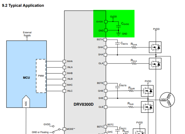
I'm using DRV8300DRGER as gate driver for inverter subcircuit of my BLDC motor controller with 3 pairs of IAUC41N06S5N102ATMA1 N-MOSFETs 

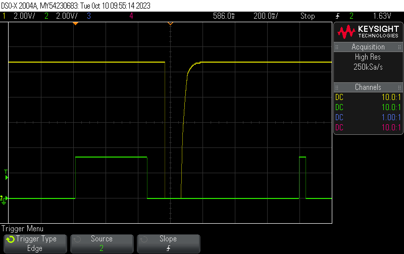
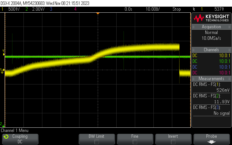
I am experiencing some strange issues. I have attached a portion of the schematic and a screenshot from the oscilloscope for reference.

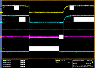
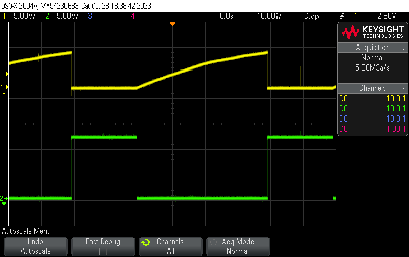
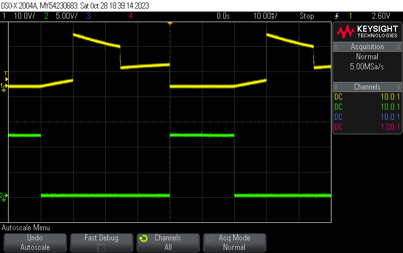
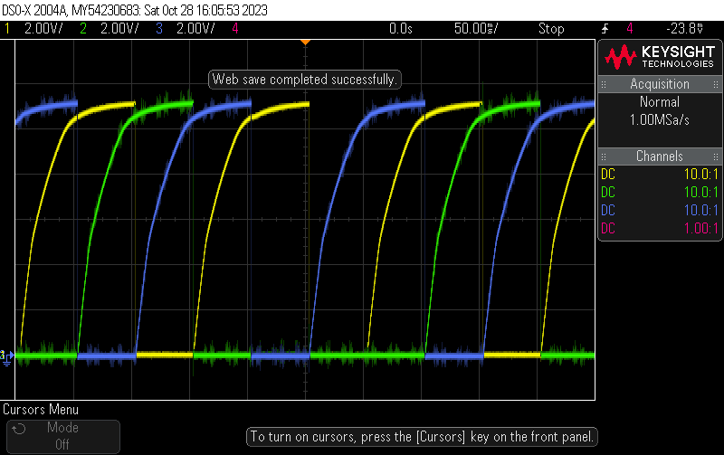
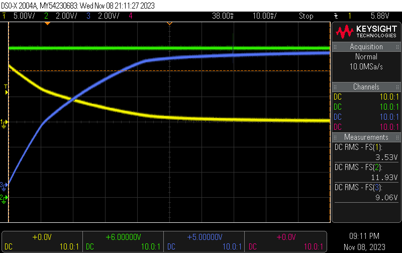
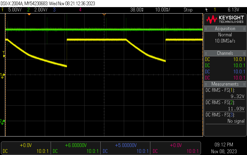
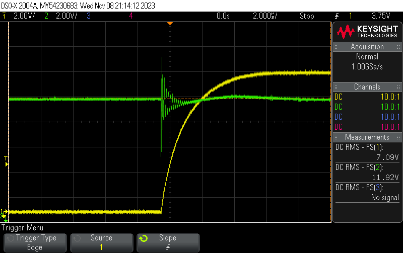
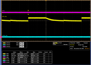
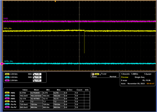
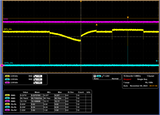
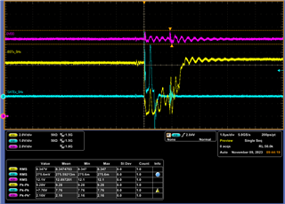
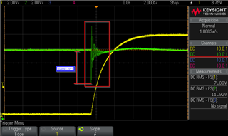
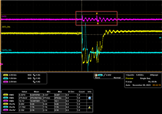
Specifically for 4 channel scope, only two phases have been measured, when driving the IC on Input A and B with low and high sides of the half bridge for BLDC, only the low side of the half bridge gate driving voltage corresponds with the PWM signal from the MCU. The yellow and blue waveforms on the screen (gate a and b on high side of the bridge) are being driven by the DRV8300, but they are not corresponding with the PWM output from the microcontroller. I have tested the code with a different design of the half bridge and it is commutating the BLDC motor without any problems.

The circuit is being tested with a Macon ec max motor and commutation is based on the delivered commutation table and hall sensor input. The PWM is created by an ESP32 WROOM 32E and directly connected to the corresponding inputs of the DRV8300 IC. During the measurement, no additional resistor for dead time was inserted, and standard time was used. No high consumption of the gate driver has been observed, and two replacements of the IC have been retested with the same results. The layout of the PCB and schematic is according to the first release of the datasheet.

For reference, the yellow line of the screencapture represents GHA, the blue line represents GHB, the purple line represents GLA, and the green line represents GLB. Additionally, corresponding PWM signals were captured using digital channels of the scope and an offset has been applied to correspond with phases.

If anyone has any additional information or suggestions, please let me know. Thank you.

  • Hi Jakub, 

    Thank you for your question and using our forum! 

    I will look into the provided info and aim to give an update on the matter as soon as I can.  

    I'll let you know if there is any additional info needed on our side. 

    Best Regards, 

    -Joshua

  • Hi Jakub,

    The driver you are using has an inverted and non-inverted mode. Based off the schematic I see that MODE pin is floating meaning you are operating in non-inverted mode, is this the mode you are intending to operate in?

    Can you please show input of the same phase you're seeing this unexcepted output?

    Regards,

    Yara

  • Hello,

    I'm attaching example of Phase A driving, signal input on INHA (green color) and gate voltage on output on pin GHA.
    As mentioned earlier, pwm is not corresponding with voltage driving each of the high side of half-bridges. This problem is same for all high side mosfet gate signals like in my original post.

    EDIT: Maybe you can share me any alternative IC which can be placed as replacement for DRV8300?

    Regards,

    Jakub

  • Hi Jakub,

    I'll need some time to discuss your issue with my team.

    Thank you,

    Yara

  • Hi, 

    Any update in my case?

    Regards

    Jakub

  • Hi Jakub,

    I'll give an update in the next 24 hours, thanks for your patience!

    Regards,

    Yara

  • Hi Jakub

    What frequency is your PWM signal? As of right now that is the only thing I could potentially think is wrong.

    How are you measuring GHA? with respect to SHA? do you know what SHA with respect to GND looks like? 

    I have tested the code with a different design of the half bridge and it is commutating the BLDC motor without any problems.

    meaning you used the DRV8300 in a different design or a completely different device? What did your schematic look like when it worked?

    Regards,

    Yara

  • Hi

    I’m using calculated 100kHz switching frequency for used mosfets, but using 1kHz, 10kHz didn’t bring any difference. 
    I’m measuring with respect to GND.

    I tested code with MCU sending PWM with right order  for used BLDC motor. I did not achieve correct work with DRV8300 on any of my design. I’ve tested now with inverting mode, it’s somehow better, but now my MOSFETs getting fried somehow, source to drain short. 
    Regards

  • Hello,

    I’m attaching more waveforms. I pull-up mode pin to GVDD and double bootstrap capacitor value.
    Furthermore, I had 10 of the DRV ICs and 5 of them died unfortunately, only this one which has been put in place of previous one work like intended. Take note that the measurement weren’t made with load.

    Greetings

    All high side mosfets gate signal above

    All low side mosfets gate signal above

    First half-bridge mosfets gate signal above

    Second half-bridge mosfets gate signal above

    Differential signal of 1 and 2 phase - output

    Output of all 3 phases.

  • Hi Jakub,

    I’m measuring with respect to GND.

    You should measure GHx and GLx with respect to SHx and SLx. If you are measureing GHx and GLx with respect to ground you could just be measuring SHx and SLx. 

    For example if GHx is 12V and SHx is 12V, the differential voltage between GHx-SHx is 0V which means that the FET is not on and the output for GHx is off.

    Regards,

    Yara

  • Helo

    I have measured now regarding to information provided. My bad for not correct measurement to gate signal. As what I can see right now the MOSFET gates are not driven at all. Vgs voltage stay at 0V despite PWM input signal or anything. 
    I’m starting to lose hope that DRV8300 will start working properly anytime. I didn’t have any issues with DRV8313. 
    If you or your team will need any more measurement of information, feel free to ask, I will provide it ASAP to resolve problems. 

    Have a good day,

    Jakub

  • Hi Jakub,

    I'm wanting to discuss some of your results with my colleagues , I'll get back to you at the start of next week.

    Regards,

    Yara

  • Hi Jakub,

    Thank you for your patience. So finding out GHx is at 0V is leading us in the right direction to solve this issue. There could be a few reason why your high side gate is at 0V. Unfortunately there are no fault pins with the DRV8300 that would tell you whether there is a fault condition or not but there are still faults that can be encountered that would result in GHx being 0V, so to rule out under voltage faults proceed with the following.

    Can you provide your waveform for GVDD? 

    Could you also provide BStx to SHx waveform? Note that if you do not have a differential probe and are using a single ended probe please measure BSTx to ground and SHx to ground.

    one last question, which side are you turning on first? High-side or low-side?

    Regards,

    Yara

  • Hi,

    I'm attaching measurements down below. If you need anything, please let me know.
    Measurements has been performed without any load (inductive or resistive).

    Greetings

    Jakub


    Green - Input voltage
    Yellow - differential signal between BST1 and SH1
    Blue - Gate 1 with respect to ground


    Green - Input voltage
    Yellow - differential signal between BST1 and SH1
    Few fast spin of motor changing PWM and commutation sequence step


    Green - Input voltage
    Yellow - differential signal between BST1 and SH1
    One step of commutation


    Green - Input voltage
    Yellow - differential signal between SH1 and Gate1
    One step of commutation

  • I'm attaching some more measurements using two differential probe. This time measurements has been made with BLDC motor also.

  • Hi Jakub,

    From your waveforms I see possibly two issues. 1.There is quite a bit of noise on GVDD and 2. BTSx might not being reaching a high enough voltage to supply pulse to GHx.

    is it possible to implement the following into your schematic to potentially reduce that noise on GVDD

    and calculate the optimal BSTx to SHx capacitor using the following section in the datasheet : 9.2.2 Bootstrap Capacitor and GVDD Capacitor Selection

    I'll be having a discussion with my team early next week to confirm and update you with anything else they might add regarding this information provided.

    Thank you for your patience.

    Yara

  • Hello,

    As you can see in original post C5 capacitor, 1uF 0805, is implemented into the design. It is 3.3mm from side of the ic and path length is about 4-4.5mm. I’m attaching photo below. 
    GVDD is 12V, which from I read is acceptable value for power supply. Power supply and oscilloscope are newly calibrated and did not produce any problem with a lot more demand testing and debugging. I’m using R&S HMP4040, Tektronix MSO5204B and Keysight DSOX2004A. 
    Nevertheless, I’ll try different decoupling capacitor. I’ve tried calculated, based on datasheet, 100nF, doubled the value and I didn’t notice any difference in performance. 

    If you will need any further information, let me know please. 

    Regards,

    Jakub

  • Thank you for all the information, I'm meeting with my team Monday so I will have an update for you then.

    Regards,

    Yara

  • Hi Jakub,

    Me and the team concluded that there are a few things that could be happening.

    As I mentioned previously, you could be encountering under voltage faults since we are only seeing issues on the high side. Have you tried operating at any other GVDD? anything high than 12V?

    Another thing to note is that you are seeing severe ringing on GVDD (from your waveform it looks like some spikes reach -20v if I am reading it correctly, this is well past the absolute maximum ratings) have you tried a larger capacitor on GVDD?

    I see in your schematic as well that there are no bulk capacitors present on PVDD?

    In your layout picture there is quite a bit of flux going across a few pins on the IC, this could potentially short the pins.

    Ultimately there are a few things in your waveforms and layout that lead me to believe the ICs you are working with could have potentially been damaged and therefore not functioning properly. Even switching out the ICs probably wont solve your issue if there is something wrong with the layout. Is this the same layout you were using when you said the DRV8313 was working?

    Have you tried using the DRV8300 EVM?

    Regards,

    Yara

  • Hi Yara,

    I can't operate at any higher voltage than 12,5V. I don't see this much of ringing on the scope, minimum voltage drop on GVDD is no more than the level of 11V. Likewise, I can use bigger capacitor and check if there will be any different, but I don't think it will change anything.

    There is 47uF electrolytic capacitor on PVDD line, it isn't visible on this part of schematic.

    I use no clean flux, which has also been cleaned out using chemicals. I did a photo before cleaning it out, my bad.

    I did not use DRV8300EVM board. Furthermore, I'll do next prototype based on different IC and inform you about result of the tests.

    Regards,

    Jakub

  • Hi Jakub,

    Sorry I may have misunderstood the waveforms, correct me if I am wrong but when I mentioned GVDD noise I was referring to this:

    as well as the noise on GHx to SHx, that seems severe enough to cause damage to the IC as well. Using the EVM in conjunction with the GUI might be beneficial in prototyping. Let me know how your further testing goes.

    Regards,

    Yara

  • Hi,

    I'd tested my design with UCC27282DR and I accomplished well enough working status of my inverter part of the design. It's a bit of pity that no resolve of the problem with DRV8300 has been found, due to that I'll proceed with work about new design based on UCC2782 IC. 
    I'll be more than happy to work, update and provide you more information about original design and more test if you would like to continue with possible finding the basis of the problem.
    You can contact me via the forum or DM.

    About mentioned waveforms, you marked that value is roughly -20V, but looking at top of screenshot there is 2V per division and ground point is way below visible on screen (mark in left bottom corner). Voltage drop on the first one is from 12VDC to 7.8VDC, with better power supply it is max of 12V to 11.5V.

    Regards,
    Jakub

  • Hi Jakub,

    It is unfortunate the DRV8300 didn't perform as expected in your layout, I still highly recommend testing with the EVM and GUI.

    I'll be closing this thread for now but please feel free to open it back up by responding, maybe providing a PCB layout for review to see if anything there could've caused issue.

    Regards,

    Yara