This thread has been locked.

If you have a related question, please click the "Ask a related question" button in the top right corner. The newly created question will be automatically linked to this question.

DRV8899-Q1:Circuit inquiry.

Other Parts Discussed in Thread: DRV8899-Q1, DRV8889-Q1, DRV8889-Q1EVM

부품 번호: DRV8899-Q1

GPT채팅으로 번역했어요

1. 수면 모드 전류를 줄이기 위해 VREF에 연결된 저항을 제거할 수 있나요?
2. 제거하면 nc로 놔둬도 되나요?
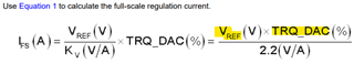
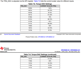
3. 이를 제거하더라도 TRQ_DAC 레지스터를 사용하여 출력 전류 설정을 변경할 수 있습니까?
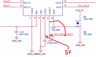
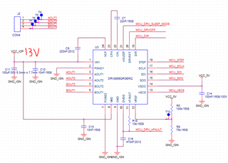
4. 현재 nSLEEP, DRVOFF, DIR, STEP, SCLK, SDI, SDO, nSCS 및 nFAULT 핀은 MCU에 직접 연결됩니다. 현재 회로는 데이터시트 8.2 일반 애플리케이션을 따르지만 문제는 MCU와 DRV8899가 모두 손상된다는 것입니다(DRV8899를 제거해도 MCU에는 손상이 없음). 회로를 어떻게 수정해야 합니까?

DIR, STEP, SCLK, SDI, nFAULT 핀에 연결됨

절전 모드, drvoff, nSCS, SDO 핀에 연결됨

  • Hi Kyuhwa, Thank you for posting your questions in this forum. I will address in the same order as you asked.

    1. I assume you are talking about both R8 and R5. Yes you can remove these.

    2. However you'll have to provide a suitable VREF input. Please keep in mind the suggested maximum input voltage to VREF is 3.3V. At 3.3V VREF with TRQ_DAC = 100% the coil currents will be 1.5A full-scale IFS.

    3. You can reduce the IFS current from 1.5A to available options using the TRQ_DAC register.


    4. This is how the DRV8889-Q1 is most commonly interfaced to an MCU. Based on your schematic VSDO = 5V rendering the SDO output level to 5V. Does the MCU support 5V logic levels? If it is not VSDO must be the same voltage as the IO voltage of the MCU. For example if the GPIO is 3.3V then VSDO must also be 3.3V. For 3.3V logic the nFAULT pull-up resistor must also be connected to 3.3V (or VSDO). 

    I also noticed a connection issue in the schematic. See below snippet. I assume the MCU_DRV_nFAULT netlist is the fault signal connection to the MCU. In the schematic it is connected directly to DVDD pin which is the internal LDO 5V output. If the MCU is not 5V IO tolerant this could also damage the MCU.  

    The schematic diagram of the DRV8889-Q1EVM can be downloaded from https://www.ti.com/lit/zip/slvc795. You can also include optional 100 Ω to 1 kΩ current limiting series resistors from the GPIO pins to these signals.

    Regards, Murugavel