This thread has been locked.

If you have a related question, please click the "Ask a related question" button in the top right corner. The newly created question will be automatically linked to this question.

DRV8462: Overheating issues

Part Number: DRV8462

Hi, 

I'm experiencing overheating with our assembly when running at these parameters: 

Step Rate = 1/256

Run Current = 60%

Standby Current = 20%

Standby Current Delay = 100ms (after 100ms, current goes to Standby Current)

Velocity = 60RPM

Acceleration/Deceleration = 100 RPM/s

The assembly was overheating (80C) after 1/2 hour of running at a duty cycle of 33%.  It was changed to roughly 14%...3 seconds off and 5 seconds on.  Afterwards, it seemed stable at roughly 56C.  


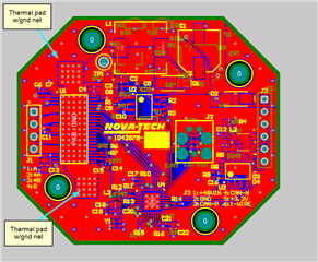
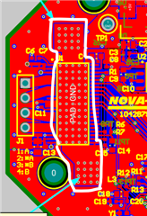
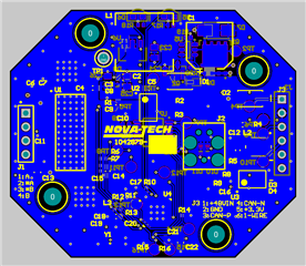
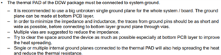
Our layout looks like this with it being 4-layer (ground and power as the 2 internal layers).  The top is flooded with poured power planes...layer 2 is ground...layer 3 is split power planes...layer 4 is flooded with a remaining ground plane.  

We even added additional areas (w/o soldermask) for an external heatsink to pull heat from both the blank and driver (using thermal pad).  ...and still, we're overheating using 1oz copper for all layers.  We have the eval board for this driver and it does get a little warm but not hot like our little board does.  Am I struggling with the amount of copper being used to dissipate heat does one think or could there be an issue with how we're driving it (a little rhetorical since you don't know our specifics)...but any help/advice is greatly appreciated!  Please ask any follow-up questions you may think of.    

  • Here is the snippet of our layout.  

  • Hi Chris,

    What is the supply voltage used? Thanks for sharing the layout. Looking at the break in the copper - see below marked with white outline - heat is not going to spread to a larger area resulting in the driver running very hot. Our recommendation would be to maximize the top layer copper and bottom layer copper area to maximize the power dissipation. You can use our EVM top layer as a reference. Altium project can be downloaded from the tool webpage. This is definitely a PCB power dissipation issue when compared with the EVM PCB. I hope this helps. Thanks.

    Regards, Murugavel

  • Hi Murugavel, 

    Thanks for the quick reply.  The voltage is 48V.  I will agree that this is a power dissipation issue.  I was revisiting the DRV8462 datasheet and layout recommendations and saw a couple of items...but first, here is the snippet of the bottom layer.  


    ...and here is the layout guidelines from TI: 


    I think we're following all the guidelines that are offered.  The only thing that I see that we're not following is having layers at 2oz...as ours are all 1oz copper planes. And again for reminder, we added an external heatsink to cover the driver and additional copper pads (using thermal pad).  

    Also, I should add that our temperature was recorded at the microcontroller (U4, bottom of the image).  

    Per your reply recommendation, I can certainly adjust the surrounding flooded plane to become ground (beyond just the area you circled).  The intent for how it is currently is to attempt to impedance match layers (power, ground, power, ground).  I don't think that altering this scheme will negatively affect our circuit performance...although we've not gotten to the CE testing specs yet. 

    Thanks. 

  • Hi Chris,

    Altering the layout will improve the thermals. Bottom layer looks okay. 2oz may be needed given the area around the driver is limited. Yes I noticed you mentioned external heatsink. Where was it placed? If on the top surface of the IC it may not be of much use. If you had a bare plated surface right underneath the device in the bottom layer and stick a heatsink on it, it would work better dissipating the heat from the chip via the thermal pad. All these should help. Thanks.

    Regards, Murugavel

  • Ok, so you're recommending that I look into moving the driver to the bottom and adjust the (above) heatsink to contact an exposed (larger) pad directly above the driver.  I can do that.  Currently, the heatsink is made to hit 3 points: the ceramic IC body and the two exposed (smaller) areas on either side of the device.  If I'm going to be throttled by my top layer and how heat is going to be held there, I'll look at a redesign.  If I had access to convection cooling (with air) I'd go that route but that's not an option.  Would you confirm again your recommendation you posted above, does that still stand as a good route (pulling heat through vias to a heatsink on the opposite side of the driver)?  

    Thanks much.

  • Hi Chris,

    Yes that's what I meant.

    You have another option as well which may be a slightly up version of this device. DRV8462 in DDV package - soon to be released. This has a thermal pad on the top of the IC for a bolt on heatsink. The IC is flipped which means the footprint will be a mirror image. Details in the DRV8462 datasheet. 100% software compatible but can support up to 10A because of the bolt on heatsink option.  

    Regards, Murugavel

  • Awesome feedback, thanks again Murugavel.  I believe this fulfills my question and i'll close this out.