This thread has been locked.

If you have a related question, please click the "Ask a related question" button in the top right corner. The newly created question will be automatically linked to this question.

DRV8402 ground pins melting


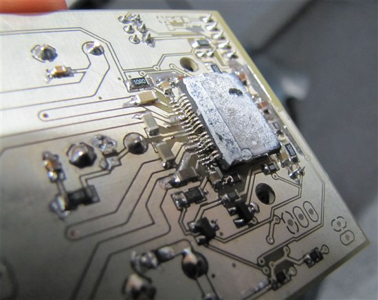
We have just implemented a prototype circuit design using the DRV8402 motor driver in parallel full bridge mode, using the schematic of the evaluation board as a guide. Upon powering up the chip operated as expected, however upon driving a load of 2A for around 5 seconds the PVDD_A/B (34 & 29) pins of the H-bridges appear to have evaporated. The PCB tracks appear to have survived undamaged, so we are quite confused as to how such damage could have occurred to the pins.

I attach a schematic of the board, and a photograph of the damaged chip. If you could advise as to a possible cause and solution for this problem I would be very grateful.

8284.mcb_rev1.pdf

  • Alexander,


    This is very interesting.  


    I will need a little more information to help you out:

    1)  What is the supply voltage you have PVDD connected to?

    2)  Where you using a motor load for your testing or just a resistor?

    3)  What did you have the "MODE" signal set at?  High or low?

    4)  Did you receive a /FAULT?

    5)  I do not see the inductors (L1,L2) in your picture...where they installed?

    6)  Can you send me PDF or gerber files of your layout?

    7)  Did you have the heatsink installed on top during your testing? 

    8)  Do you have another board to try to verify there wasn't some short on this board?


  • Hi Ryan, thanks for your prompt reply. To answer your questions:

    1) The supply voltage was 48v

    2) We were using a motor load

    3) MODE was M3: 0, M2: 1, M1: 0 (Parallel full bridge with cycle-by-cycle current limit)

    4) We didn't receive a /FAULT or /OTW prior to the failure

    5) The inductors were installed, they are on the opposite side of the board and hence not shown in that photo

    6) This interface will not allow me to upload the gerber files, so I have sent them to your TI e-mail address

    7) we had a large heatsink installed with thermal paste

    8) We haven't yet put together another board, so can't check this - however I'm not sure how a short on the board could cause this - we were monitoring the total current consumption and as stated before, it was around 2A


  • Alexander,

    I think the answer to my first question gives me the best clue. 

    If you put a scope probe on the outputs, you will see some large peak voltages during the switching transients.  Try backing the supply down to 36V and measure the peak voltage. 

    To limit these peaks and allow operation at 48V, I would recommend adding some snubbers on each output.  3.3ohm+10nF to GND from each output as close to the IC as possible.  You can check the scope captures before and after adding these at 36V to get an idea on how well they work on your board layout.

    One other thing to note is there should be an electrical connection from the heatsink to the board GND.  The exposed pad on the top of the package is the substrate connection to the IC.  You don't need to use a silver filled compound or anything as the heatsink pressure usually is enough to squeeze out the thermal compound and make an electrical connection to a bare, aluminum heat sink (if using an anodized heat sink, scrape off the connection to the PowerPAD to expose bare aluminum).  The screws that are used to tighten down the heat sink on top of the package should be electrically connected to GND to complete the circuit and ensure the substrate is grounded.

    I think your main problem is voltage spikes and this can be verified by doing some testing at a lower voltage.