This thread has been locked.

If you have a related question, please click the "Ask a related question" button in the top right corner. The newly created question will be automatically linked to this question.

DRV8962: Hi-Z Resistive Load

Part Number: DRV8962
Other Parts Discussed in Thread: DRV8955

Hi. We have a non-typical application that drives a capacitive load using the DRV8962 and a power op-amp. The DRV8962 output and the op-amp output are connected in parallel to the capacitive load, with a resistor in between the DRV8962 and op-amp. See picture below for general connection.
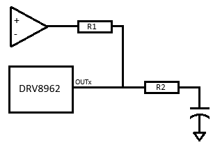
In general this setup is working fine. The op-amp controls the majority of the output signal to the capacitive load while the DRV8962 fires a high or low FET at certain signal transitions. When the capacitive load is held at a steady state voltage, the DRV8962 will be disabled (ENx low) and the op-amp holds the output voltage. The problem we are having is that in this state we are seeing about a 0.2V to 0.5V drop on R1. This is causing unnecessary heat dissipation on both R1 and the op-amp. As the capacitor is fully charged at this point, the only avenue for a resistive load would be the DRV8962 in its hi-Z state. 

Additionally, if we put the DRV8962 in sleep mode, driving nSLEEP low, the resistive load is eliminated and there is no voltage drop on R1. Excessive heat is eliminated.

The relationship between the steady state voltage and voltage drop on R1 isn't as linear as I would expect so we are having some trouble determining the resistive load of the DRV8962. Do you have any details on the behavior/impedance of the DRV8962 OUT signals while disabled? We were not able to find any details in the datasheet. Thanks.

  • Hey Thomas,

    Ahh interesting.  Can you post a scope capture of the R1 drop? I'd like to see if it starts high and decreases like a capacitor discharge circuit, or if it could be due to an internal protection diode or something.  

    Also what are the values of R1, R2, and what model op-amp?

    Best,

    Jacob

  • Hi Jacob,

    Our thought was that it could be something with the FET diodes as well, but not sure how. We will typically have R1 as 10R and R2 at 3R. Additionally we use 36V to power the DRV8962.

    I don't believe R2 will have much impact on this as we have changed it throughout testing for other purposes. We also removed the capacitive load with no impact to behavior. 

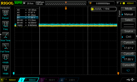
    See below for a couple scope captures. The first is with the /SLEEP low. No current flow or heat dissipation here.

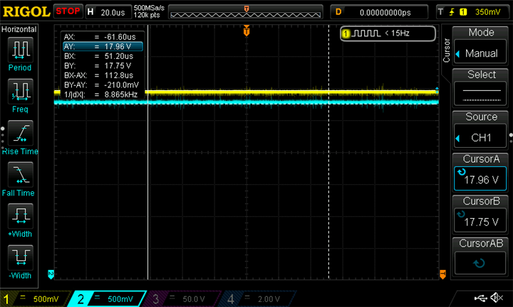
    Once I switch /SLEEP high and keep ENx low, I get a small voltage drop across the resistor. See below.

    Let me know your thoughts. Thanks.

  • Hi Thomas,

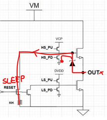
    This leakage can be attributed to the internal circuitry of the H-bridge. Below is a high level circuit diagram of the internal gate drive. You may notice a Zener diode from OUTx to the gate of the HS output FET. This is to ensure the source and gate of the HS FET are not floating while Hi-Z. While ENx is 0 the HS_PD FET will be conducting and serve as a current sink path to the Zener diode from OUTx. While the device is in sleep mode the HS_PD FET does not receive drive however another FET shown with RESET conducts via an approx. 50k resistor resulting in a much smaller leakage, albeit a current leakage path from the OUTx via the Zener. I hope this explains the behavior observed by you. You may have to work around this. Thanks. 

    Regards, Murugavel

  • Thanks Murugavel. This is good information. We'll see if we can work around this.

  • HI Murugavel. A quick follow up question. Does the DRV8955 have the same sort of connection on the half bridge outputs?

  • Hi Thomas,

    While it may not be exactly the same type of circuit I do expect something similar for the HS FET with a current leakage path towards GND potential on the OUTx. So yes with regards to leakage path.

    Regards, Murugavel