This thread has been locked.

If you have a related question, please click the "Ask a related question" button in the top right corner. The newly created question will be automatically linked to this question.

DRV8718-Q1: DRV8718 software configuration

Part Number: DRV8718-Q1

Hi team,

Customer is doing software eval of DRV8718, and below is the command

Write 87 to 0X07 (IC_CTRL1)

Write 12 to 0X08 (IC_CTRL2)

Write 12 to 0x26 (CSA_CTRL1)

Write 00 to 0X09 (BRG_CTRL1)

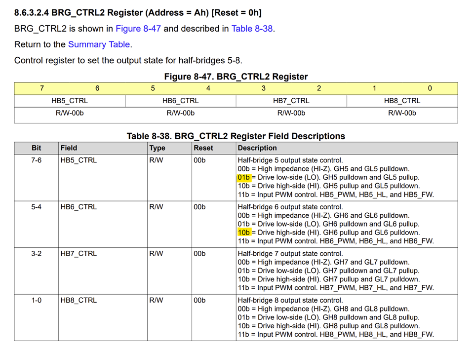
Write 00 to 0X0A (BRG_CTRL2)

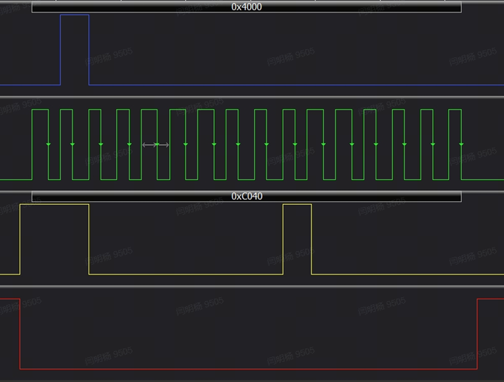
Then they connect half bridge 5 and 6 with a 1 ohm power resistor to simulate the motor load, enable the bridge by write 60 to 0X0A, there's no voltage change. Is there any step missing?

Thank you

Scarlett

  • Hi Scarlett,

    The sequence looks okay to me. So the LS should be on in HB5 and HS should be on in HB6. What are the values read from the IC_STAT1, VDS_STAT2 and VGS_STAT2? One important point to keep in mind. 1 ohm power resistor is not a simulator for motor load although the motor may have 1 ohms DCR. BDC motor has an inductance and when the motor runs it has a lot of BEMF to reduce the inrush current. 1 ohm does not do all those. At the minimum the simulation should be a higher resistance like 10 ohms and a series inductor to simulate an equivalent running current of the motor not the starting inrush or stall current of the motor. 1 ohm will result in overcurrent and could damage the output FETs.

    Regards, Murugavel

  • Hi Murugavel,

    Thanks for your support. Customer read IC_STAT3 and the result is 0XC008, so the SPI communication should be correct. VDS_STAT2 and VGS_STAT2 also normal, no OV OC. However, the IC_STAT1 returns 0XC040(bit 7 abnormal), does it mean there's SPI fault that stops DRV8718 output? Please see the record below

    Thanks

    Scarlett

  • Hi Scarlett,

    IC_STAT3 = 0xC008 read correct yes. But IC_STAT1 = 0xC040, BIT6 = 1 which means POR has happened. This is normal behavior, the first time device is powered up POR bit will be set. I don't see any other error happening. The device responses looks right.  

    After writing 0x87 to 0X07 (IC_CTRL1) which issues a CLR_FLT the POR bit in IC_STAT1 will clear. This can be verified. 

    I have a question with IC_CTRL2 in the first message you said was written with 0x12. How is the DRVOFF/nFLT pin treated in the circuit? Writing 0x12 to IC_CTRL2 means this pin is treated as DRVOFF global driver disable if the pin is pulled logic high. In this case this pin must be pulled low to enable the drivers - it does have an internal pulldown resistor. Typically this pin would be used as nFLT (nFAULT). For this IC_CTRL2 must be written 0x52, which makes the fault pin open drain output. Please check with this. I think this may be the issue. If the problem persists please share the schematic. Thanks.

    Regards, Murugavel 

  • Hi Murugavel,

    Since this is public e2e I'm sharing customer schematic to you through email. You can close this thread.

    Thanks

    Scarlett

  • Hi Scarlett,

    Please close this thread at your end. Thanks.

    Regards, Murugavel