This thread has been locked.

If you have a related question, please click the "Ask a related question" button in the top right corner. The newly created question will be automatically linked to this question.

DRV8302: GVDD and Charge pump charging and discharging working principle

Part Number: DRV8302
Other Parts Discussed in Thread: DRV8328

Hi Team,

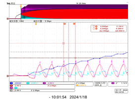
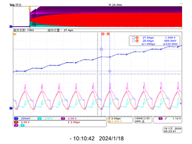
The test condition is 24V, and the waveform collected during the test is shown in the figure below. The amplification part is the GVDD startup stage. CH1 is the GVDD waveform, CH2 is the CP1 terminal, and CH3 is the CP2 terminal. Is the voltage increase of GVDD due to the charge and discharge of the CP capacitor? The customer considers that the reference voltages of the two are different, and he wants to know how to increase the voltage? Could you share and explain the working mode of Charge pump and GVDD?


Regards,

Annie

  • Hi Annie, 

    Allow me to look into this topic and follow up within the week. 

    Thanks and Best Regards,

    -Joshua

  • Hi Joshua,

    May I know is there any update for this thread?

    Regards,

    Annie

  • Hi Annie,  

    I will follow up tomorrow with an update on this inquiry. 

    Best Regards, 

    -Joshua

  • Hi Annie,

    Can you clarify further the behavior observed on GVDD? What voltage does GVDD start at on device power up and what is the max voltage reached? 

    GVDD is internally generated and can supply up to 30mA externally and can ripple in response to the charge pump switching, but should be relatively linear around 11-12V, not increasing past the abs max of 13.2V.

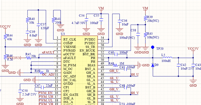
    Can you also provide the schematic used to better understand the application connections? 

    Thank You and Best Regards,

    -Joshua

  • Hi Joshua,

    Power up the device and observe that the GVDD voltage gradually increases from the starting voltage 0V to the maximum voltage of about 11V. GVDD is generated internally, but what circuit and principle is used to charge the 11V voltage to 11V? The following two waveform diagrams, the left picture is the initial stage and the right picture is the charging stage. The blue one is the GVDD voltage, and the red one is the charge pump CP capacitor charging voltage. It can be seen that the CP capacitor is repeatedly charging and discharging, but the maximum voltage is only about 4V. So where does the voltage of GVDD greater than 4V and the voltage charged to 11V come from?


    The schematic diagram of the 8302 peripheral circuit is as follows:

    Regards,

    Annie

  • Hi Annie, 

    Thank you for the clarification and additional information.  

    Please allow me to look over this and further a suggestion/answer after review by the end of the week. 

    Best Regards,

    -Joshua

  • Hi Joshua,

    It would be helpful if you could get back to me regarding this question.

    Regards,

    Annie

  • Hi Annie, 

    I do not yet have the specifics of how the internal gvdd for this device is generated,  but believe it may be similar to the DRV8328 where the GVDD is generated from an internal LDO for certain supply voltages, and generated by the charge pump regulation for lower values:

    The charge pump works on the principle of charging up the charge pump capacitor to the reference voltage (pvdd) and discharging in sequence during operation,  allowing for a relatively constant output.

    Does this help answer the question?

    Best Regards, 

    -Joshua