This thread has been locked.

If you have a related question, please click the "Ask a related question" button in the top right corner. The newly created question will be automatically linked to this question.

DRV8312: EMC emission issue

Part Number: DRV8312

Hi Team,

My customer have identified that the motor circuitry is a significant contributor to EMC emissions radiating from their device.


They've been investigating the motor driver circuit and they suspect that the DRV8312 is experiencing parasitic turn-on, causing current shoot-through. This issue could explain the high emissions.


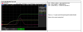
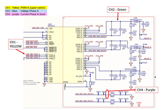
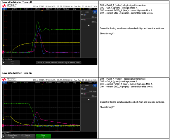
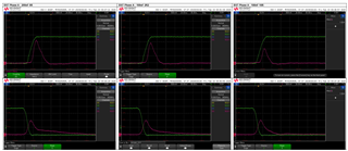
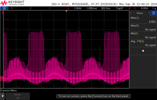
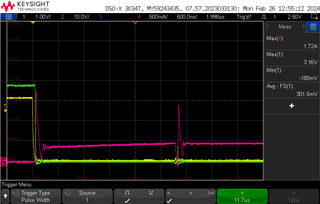
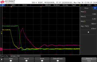
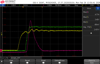
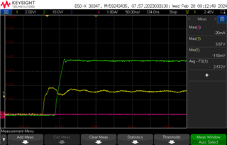
Below are the turn-on and turn-off waveforms for the bottom Mosfet (Phase A).

The motor is not connected, the micro is applying a 50% duty 30kHz PWM to PWM input phase A only.

Since there is no load, the diodes are not conducting, they don’t expect any reverse recovery.


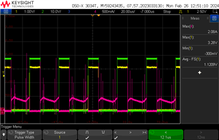
For the turn-off (bottom Mosfet), they see a 1 Amp peak current. However, for this condition, they would not expect any current to flow through (unless they're missing something).

Could this be a parasitic turn-on, lifting the gate voltage caused by high dV/dt (possibly induced by our layout)?


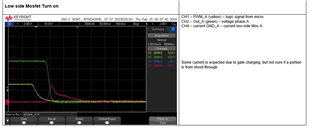
For the turn-on, they see a smaller peak current, which I understand to be the gate charge (and plus some shoot-through as well?)


Unfortunately, they don’t have access to the gate voltage to see if it is going above the Vgs threshold.


Can you please help us understand this turn-off waveform?


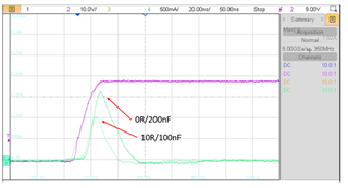
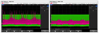
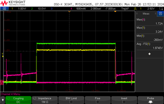
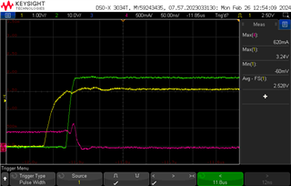
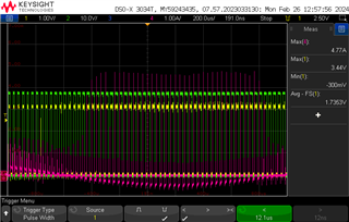
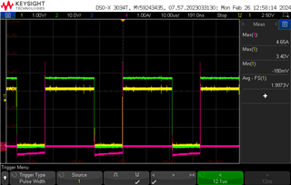
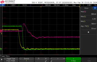
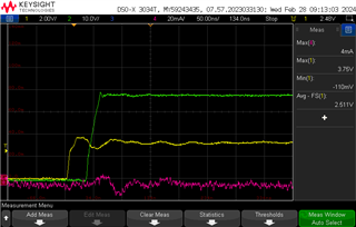
they did the same measurement for phase B, but less intrusive, using a voltage probe across the shunt resistor and they see the same peak current.

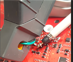
(instead of cutting the track and adding a wire-loop for the current probe which can add inductance to the circuit)

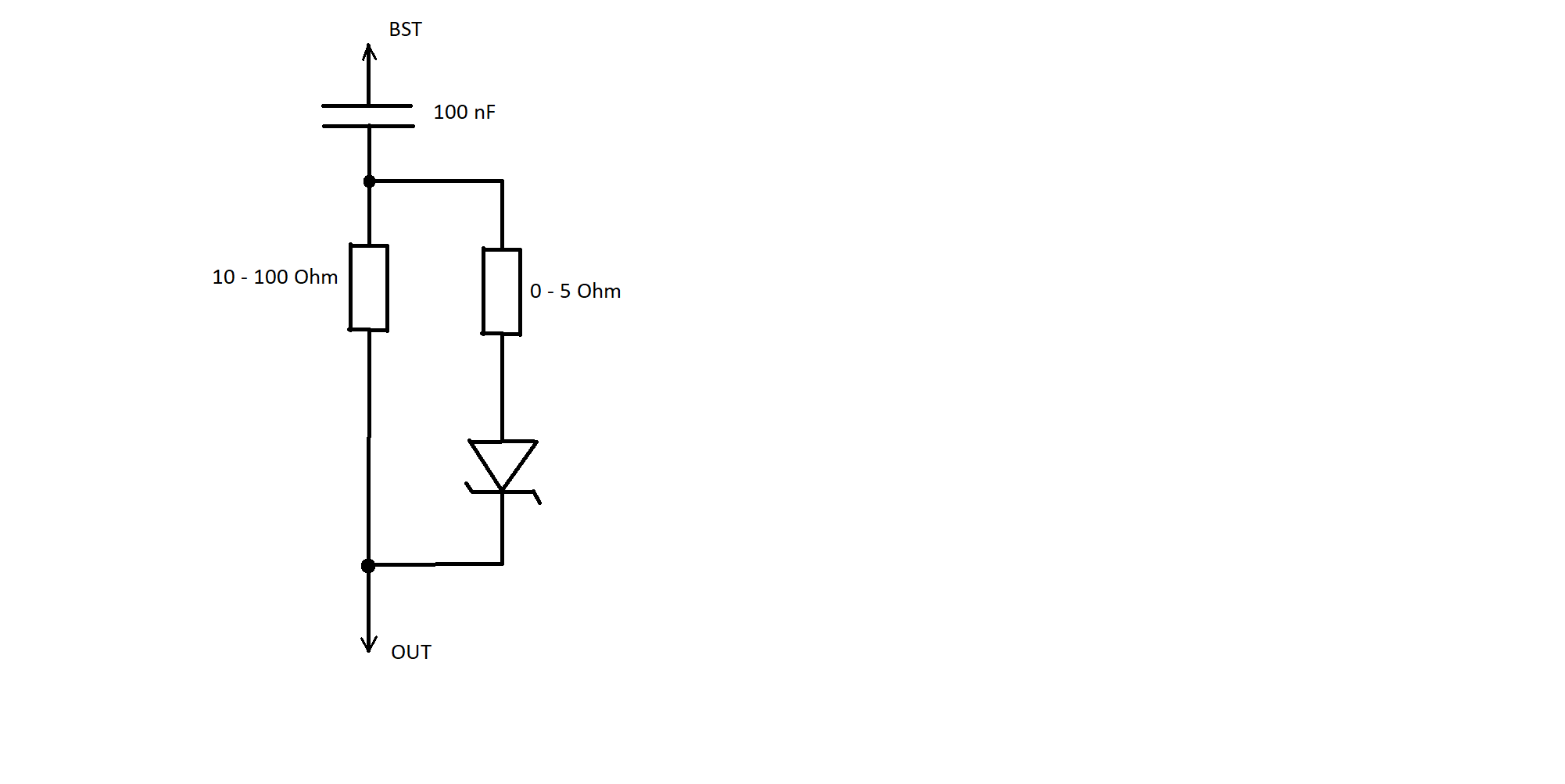
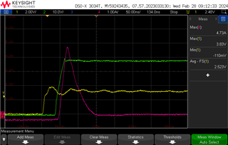
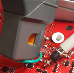
There are snubber capacitors connected to phase A, B, C to GND, these seem to help emission.

For the waveforms above, they removed the capacitors to eliminate the possibility of shoot-through caused by them.

Please kindly advise, thank you and appreciate your time.

Best Regards,

Ernest

  • Hello,

    Thank you for your E2E post. I'll look into your issue and provide an update by the beginning of next week.

    Regards,

    Yara

  • Hi Yara,

    I want to share new waveforms. Customer managed to cut the track and add a current probe to the upper switch as well.

    They can observe that current is flowing simultaneously on both high and low side switches. Please see captures below.

    Notes:

    • No load connected;
    • PWM phase A only, 30kHz 50% duty;
    • Turn off bandwidth limitation. Found that scope had bandwidth limitation enabled on previous captures, these new captures are not bandwidth-limited;
    • Adding a wire loop to PVDD_A adds ringing to the system due to the additional inductance.

    Is this expected?

    Best Regards,

    Ernest

  • Hi Ernest,

    Thank you for the additional information. When was this issue noticed? Was there a time when the system was working without issue? If so what changed since then?

    I don't think the behavior you are observing is to be expected. I'm trying to discuss your issue with my team to try and debug. I'll give you and update by the end of this week.

    Thank you

    Yara.

  • Hi Ernest,

    Could you try to run driver with just single 100nF bootstrap capacitors and add to them resistors of around 2,2 Ohm in series?

    Regards,

    Grzegorz

  • Hi Yara,

    Customer product has always struggled with emissions. They have virtually no margin to the limits.

    They have been getting away with small filter tweaks but never understood the root cause.

    Their goal is to find the source of the emissions/root cause.


  • Hi Grzegorz,

    Thanks for your response. 

    Customer tried your suggestion (2R2 resistor) and can see a slight reduction in the “shoot-through current”.

    Then, then tried a 10R resistor and the difference is very significant.

    Please see the waveforms below.


    They run the same condition:

    • No load connected;
    • PWM phase A only, 30kHz 50% duty;
    • Wire loop for current measurement on lower side Mosfet only.


    You can overlay the captures to see the difference:

    The waveform below is the 10R waveform on top of the 0R condition. Voltage of phase A, and current through the low-side mos.


    • Is this a parasitic turn-on?
    • Is there a way to eliminate completely this current?

    Customer did another test with motor connector. 

    They have two waveforms with the motor running at 2krpm very light load (their motor spins at 32krpm maximum).


    You can see that there are random peaks of 4.7 amps on the left image.

    When they add the 10R to the bootstrap the peaks go away.

    They believe the 10R is causing the upper Mosfet to turn on slower, reducing the parasitic turn-on.


    CH2 – Out_A (green) – voltage phase A

    CH4 – current GND_A (purple) – current low-side Mos A.


    Best Regards,

    Ernest

  • Hi Ernest,

    Thank you for sharing all data.

    Adding series resistors of around 2R2 to bootstrap caps is a quite common practice to reduce EMI in DC/DC converters.

    "Is this a parasitic turn-on?" - I guess not, PVDD is just 38V while DRV8312 is 70V rated. I would rather suspect some shoot-through you mentioned earlier caused by very short dead time - according to datasheet it is around 5.5ns.

    "Is there a way to eliminate completely this current?" - If increasing value of bootstrap resistor and slowing down HS Mosfet turn on works well then maybe it is a way to do it.

    Increasing further the value of series resistor alone may bring problems with bootstrap capacitor charging process.

    I would try to use circuit below with some high speed Schottky diode like PMEG3010AESB. If resistor that is in series with diode does not improve EMI then it could be omitted. 

    "You can see that there are random peaks of 4.7 amps on the left image." - It may be helpful to see waveforms of these current peaks together with voltage output phase and PWM signal at 20-50ns/div.

    I do not have an experience with DRV8312 but taking a look at its datasheet I think it is a really high speed Mosfet driver (rise/fall times around 14ns) and its footprint may cause PCB layout design challenging to meet EMI limits.

    PS. PCB layout may play some role in above mentioned problems as well. PMEG6010AESBYL would be a safer choice.

    Best Regards,

    Grzegorz

  • Hi and

    My name is Ede, I am Ernest's customer. Thank you for your help so far on this matter. 

    Please see the waveforms below with motor running.
    I noticed that the big current spikes( > 4 amps) are happening when the current is negative in the bottom Mosfet.
    These big spikes do not happen when current is positive, reverse recovery is ~ 1.7 Amps only.
    I expect reverse recovery from the diodes, but I would expect the same level for upper and bottom diodes.

    And as I shared previously, I can see that these 4 amps peaks become less frequent (but still randomly present) with light loads.
    Perhaps, this indicates that is something related to parasitic inductance, as the dI/dt changes with load.
      

    Notes for waveforms below:

    • Motor spinning at 10k rpm.
    • Input power 5 W.
    • Bootstrap 200nF / 0R.
    • Snubber capacitors removed from motor’s phases.

     CH1 – PWM_A (yellow) – logic signal from micro

    CH2 – Out_A (green) – voltage phase A

    CH4 – current GND_A (purple) – current low-side Mos A.


    Overview  - 10000rpm


    Positive cycle overview


    Positive cycle - Turn off / Turn on overview


    Positive cycle - Turn off


    Positive cycle - Turn on


    Positive cycle - Turn on – zoom in


    Negative cycle overview – note 4 amps peak during negative cycle


    Negative cycle - Turn off / Turn on overview


    Negative cycle - Turn off


    Negative cycle - Turn on


    I will try your suggestion of slowing down HS mosfet, but I would be keen to understand the mechanism behind this behaviour, as this should not occur in the first place.


    Thank you very much.
    Ede.

  • Hi Ede,

    Thank you for providing all data.

    Can you tell what is BW of your current probe? Was BW limit set on your oscilloscope during measurements and voltage probe (used for phase voltage measurement), was it set to 1:1 or 10:1 range?

    Phase voltage waveform looks very clean for problems that you experience.

    Could you also tell at what frequencies you have EMI problems?

    PS. Do you know maybe time delay of your current probe?

    Could you make also some measurements of noise picked up by current probe by placing probe in the same position but not closing it on wire loop?

    Best Regards,

    Grzegorz

  • Hi Grzegorz,

    Here is the spec of the gear I'm using:

    Current probe:

    • HIOKI 3273-50 (50 MHz, 30 Amps).
    • Not sure about the delay, but rise time is 7ns or less. Probe has been calibrated recently.
    • Scope is set to 0.1V/A.

    Voltage probes:

    • Keysight N2843A (500MHz, 10:1) 
    • Scope sets automatically 10:1 range

    Scope:

    • Keysight DSOX3034T (350MHz, 5GSa/s)
    • Acquire mode: Normal
    • BW limit for all channels OFF (the very first captures I sent to Ernest had it on, but then I turned it off after realizing it was enabled).

    Could you also tell at what frequencies you have EMI problems?

    - Motor noise is very significant between 100MHz and 200MHz

    Could you make also some measurements of noise picked up by current probe by placing probe in the same position but not closing it on wire loop?

    Not sure if I understood correctly, but here is what I did: I don't see any noise, even when the vertical scale is set to 20mA.

    Please let me know if this is the correct way of checking noise pick up. I can re-do it if this is not what you wanted it.

    Notes:

     CH1 – PWM_A (yellow) – logic signal from micro (ground of the probe not connected, thus the ringing).

    CH2 – Out_A (green) – voltage phase A

    CH4 – current GND_A (purple) – current low-side Mos A.

       1A/div


     1A/div

     20mA/div

    Thank you very much.

    Ede.

  • Hi Ede,

    Thank you for sharing all additional information.

    According to datasheet HIOKI 3273-50 has delay time of 16ns. Voltage probe N2843A with 1,3m cable has probably delay time of around 6ns. Then current waveforms are probably around 10ns late to voltage waveforms.

    It means that current waveform rising edge is roughly in phase with voltage waveform rising edge (case with current peak over 4.5A).

    I guess that BW of probes, oscilloscope settings and good setup mean that all above measured waveforms are pretty real ones.

    "Not sure if I understood correctly, but here is what I did: I don't see any noise, even when the vertical scale is set to 20mA." - It is what I meant. I suspected that current probe circuitry picks up noise from other 2 half-bridges ("Positive cycle overview" waveform) but apparently it is not the case.

    "Positive cycle - Turn on – zoom in" - If we move current waveform 10ns back then beginning of its rising edge will start before output voltage starts to fall. Additionally we can see small voltage bump around 10ns long just before output voltage starts to fall (HS Mosfet body diode voltage drop). I think all that means that current peak of 1.68A is caused mainly by HS Mosfet body diode reverse recovery.

    "Negative cycle - Turn off" -  If we move current waveform 10ns back then beginning of its rising edge will be where output voltage starts to rise. There is no any voltage drop just before output voltage starts to rise and there is some small dent in rising output voltage at 15V. I guess HS Mosfet started to turn on before LS Mosfet fully turned off and caused LS Mosfet conduct again. ""Is this a parasitic turn-on?" - I guess not" - probably I was wrong, I guess it is a parasitic turn-on caused by very short dead time.

    Voltage output waveform looks very decent for a shoot-through event (probably it lasts too short to cause any bigger problems), there is some small overshoot with frequency that probably fits within 100-200MHz range.

    Wire loop between LS Mosfet source and sense resistor, probably around 1,5cm in diameter adds around 30nH of parasitic inductance to traces and sense resistor parasitic inductances. There is some chance that excessive parasitic inductance between LS Mosfet source and GND might disturb LS Mosfet switching process. 

    "Positive cycle overview" - I wonder how other 2 phases can disturb Phase A LS Mosfet current waveform so much. If it is not caused by noise picked by current probe then I guess it might be caused by not very good PVDD_X pins decoupling or PCB layout.

    Maybe it would be worth to check PCB layout and PVDD_X decoupling for any possible improvements. Current sense resistor itself can have significant parasitic inductance unless it is some kind of low inductance type. I would make some trials without wire-loop used for current probe that introduces large parasitic inductance into Mosfet half-bridge. If someone does not have spectrum analyzer he/she can use oscilloscope to measure voltage ringing amplitude on sense resistors and output phases. Ringing and EMI usually rises with higher output currents and higher di/dt. Simple near field probe can be made with 10:1 oscilloscope probe by connecting grounding clip to probe tip to check EMI close to driver and output cables (oscilloscope channel set to AC and around 5-20ns/div).

    I do not know if better PCB layout could limit the problem with shoot-through but there is a chance that it may help with EMI. If it does not help then slowing HS Mosfet down could be a solution, luckily it is not LS Mosfet that would need to be slowed down because it seems that there is no any access to its gate driver.

    Best Regards,

    Grzegorz 

  • Hi Grzegorz,

    Thank you for the insights.

    I also don't understand the "noises" from the other 2 half legs. This is something I need to investigate further.

    I agree with your analysis of the "Positive cycle - Turn on – zoom in" and "Negative cycle - Turn off". What is odd to me is the huge difference between 1.68 A peak recovery during the positive cycle and the 4.77 A for the negative cycle. This 4.77A must be a combination of recovery + shoot-through. 

    I will investigate the negative cycle and see how the current is flowing, perhaps that is telling me something (parasitic inductance in this path).

    I will review our layout and the components used in our design, as per your suggestion.

    Is there any demo/application board that I could use as a reference?

    The first thing I wanted to establish when I contacted Ernest was to confirm whether the waveforms were abnormal. You helped me to confirm that. Thank you. Now I will dedicate some time to finding the root cause or a remedy for it.

    Thank you.

    Ede.

  • Hi Ede,

    It looks like eval board used to be available but not any more

    https://www.mouser.pl/ProductDetail/Texas-Instruments/DRV8312-C2-KIT?qs=%252BG2H6gVb6iyOUG85oF%2F6iQ%3D%3D

    https://de.mathworks.com/help/ti-c2000/ug/mcb_hw_28069.png

    You use just 2 sense resistors with GND_C pin grounded directly to GND. Instead of Phase C I would ground Phase A or B, it would give some extra space

    at the bottom of DRV8312 which is more crowded than upper part of the IC. It should allow to shorten traces between GND_X pins and sense resistors. 4-layer board should also help to limit parasitic inductances.

    Best Regards,

    Grzegorz

  • Hi Ede and Grzegorz,

    Thank you Grzegorz for you expertise and insight on the issue!

    Ede, to review your layout typically we recommend looking at the hardware files of the EVM, however it looks like this device didn't really have an EVM rather a "C2-KIT" which I don't believe we even release anymore and I cant seem to find the files.

    We do have a Best Practices for Board Layout of Motor Drivers that would be a great resource to conduct your layout review with.

    Let me know if you have any more questions

    Thanks!

    Yara