This thread has been locked.

If you have a related question, please click the "Ask a related question" button in the top right corner. The newly created question will be automatically linked to this question.

DRV8703-Q1: How do I get PWM

Part Number: DRV8703-Q1

Hi Expert,

I encountered some difficulties in the debugging process.

Now I can do SPI communication , but I can't get PWM.

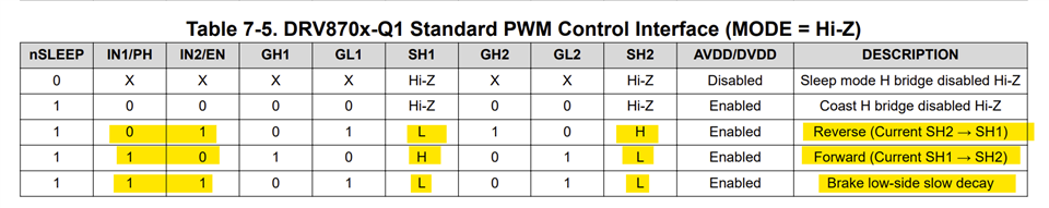
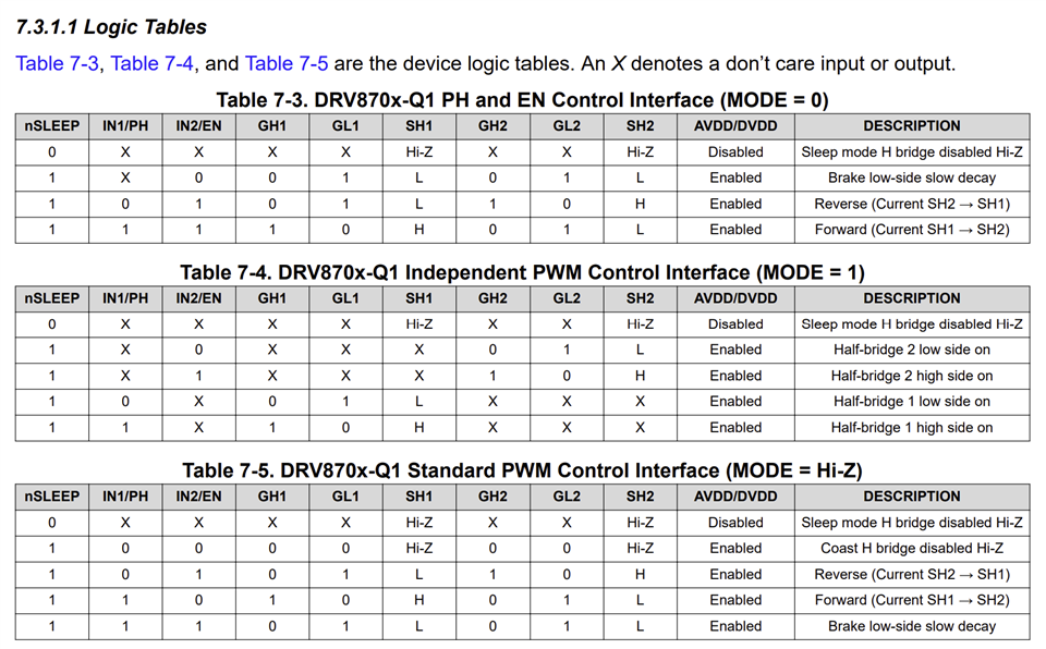
According to my understanding,as long as I set "nSLEEP" = 1,"mode" = HiZ , "IN1" = 1 "IN2" = 0, I will get PWM.(Please remind me if I'm wrong)

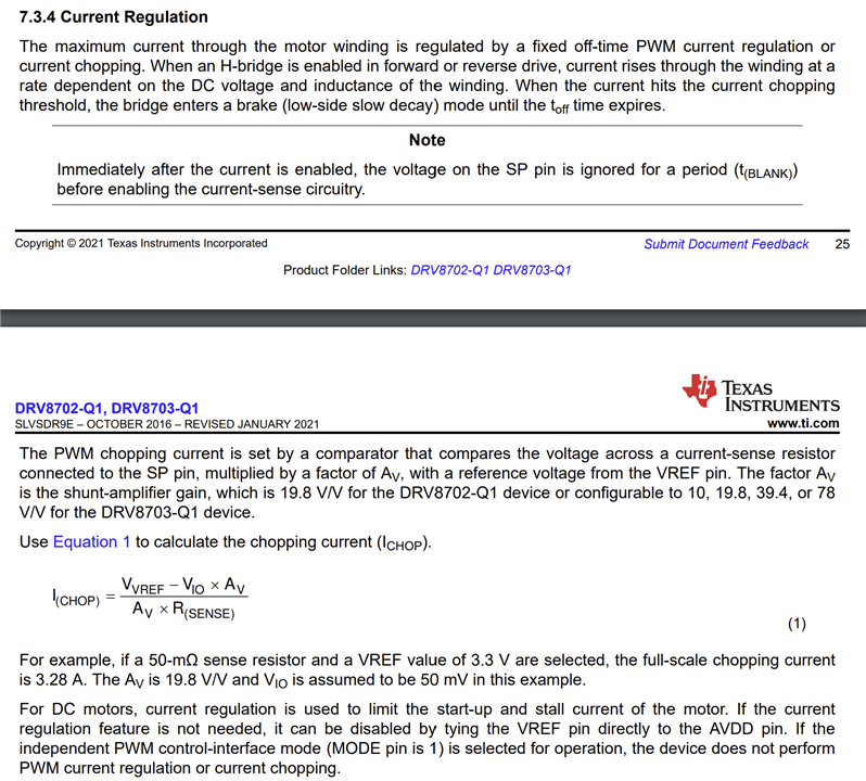
But  I set "nSLEEP" = 1,"mode" = HiZ , "IN1" = 1 "IN2" = 0 , VDS and GDF Status Register = 0x04.And no matter how I configure it , VDS always overcurrent.I wonder if I missed something

BR,

Huan Yin

  • Hi Huan,

    Thank you for posting in this forum. In order for the device to power up in PWM input H-bridge mode the MODE pins must be HiZ while nSLEEP = 0 and transitions to 1. Then, when nSLEEP = 1 the device wakes up and latches the MODE status (input HiZ) to PWM input H-bridge mode. In this mode of bridge control as shown in Table 7-5, one of the inputs must be HIGH (IN1) and the other input (IN2) must be input with a PWM input with variable duty cycle to vary the speed of the BDC motor at the output. When IN2 is HIGH and IN1 is input with PWM the motor will spin in the opposite direction. What is the input PWM frequency and duty cycle provided to the input during the tests?

    When PWM input = 0 the motor will be driven. When PWM input = 1, both IN1 and IN2 will be HIGH resulting in low side FET slow decay of the current in the motor winding. This process happens for every PWM on/off period. The motor can be driven with 100 % speed without using a PWM input and instead making one of the inputs LOW while the other input is HIGH.  

    Was current regulation enabled and used during the tests? What were the settings for current regulation used and the sense resistor used? What was the supply voltage used? What is the type of load connected to the output? 

    VDS and GDF Status Register = 0x04 means L2_VDS low side FET has VDS error. The default VDS setting is 0.96 V unless you changed it to a lower value. If the FET's you were using had 2 mΩ Rdson, 0.96 V would mean 0.96/0.002 = 480 A flowed via the LS2 FET which is abnormally high current - not really a possibility. What is the Rdson of the FET used. Were you able to measure the current spike through the load using a current probe? It will be helpful if you could share the current waveform taken while the VDS overcurrent is reported by triggering the capture with the nFAULT pin (requires pullup). If we could see the schematic around the driver and the output FETs it will help us with the debug. Thanks. 

    Regards, Murugavel 

  • Hi,Murugavel

    You said " one of the inputs must be HIGH (IN1) and the other input (IN2) must be input with a PWM input with variable duty cycle to vary the speed of the BDC motor at the output.". I can use SPI communication to make IN1 HIGH, but I don't know how I input a PWM input with variable duty cycle in IN2.Maybe I need another chip to generate PWM,then PWM is connected to the IN2 as input? I thought DRV8703 could generate PWM on its own.It seems that I misunderstood.

    The supply voltage is 12V, and the type of load connected to the output is a DC speed reduction motor.

    I made some changes to the hardware.Although the motor was successfully turned,FAULT Status Register = 0x88(VM undervoltage).The 12V voltage first becomes 6V and finally reaches 11V, and the current also reaches the maximum limit of 0.2A.I'm going to configure a PWM output and see what happens

    BR,

    Huan Yin

  • Hi Huan,

    Yes the PWM is usually generated by a microcontroller. This is required only if you'd want to have a PWM speed control. Applications that don't need speed control can be controlled by SPI IN1 and IN2. The DRV8703 does not have internal PWM to drive the motor. 

    Our EVM for this device https://www.ti.com/tool/DRV8703-Q1EVM?keyMatch=DRV8703-Q1EVM uses a TI microcontroller to generate PWM for controlling the motor speed. The hardware files including the EVM schematic can be downloaded from https://www.ti.com/lit/zip/slvc675. The EVM firmware source code can be downloaded from  https://dr-download.ti.com/secure/software-development/support-software/MD-KF25Q3LqZz/01.00.00.0A/slvc673a.zip

    You said "I made some changes to the hardware. Although the motor was successfully turned, FAULT Status Register = 0x88(VM undervoltage).The 12V voltage first becomes 6V and finally reaches 11V, and the current also reaches the maximum limit of 0.2A.". Did the power supply have a current limit set? BDC motors have a large inrush current during startup which can reach 10's to 30's of amps until the motor reaches speed and generate enough back EMF (BEMF) to oppose the current flow until it reaches a equilibrium steady state current when the motor runs at a fixed speed. A current limited power supply will not able to sustain output voltage at these high currents and the driver will report a VM undervoltage. A VMUV will also disable the output drive during the UV situation so the motor coil will not reach the desired current to startup and run.

    "I'm going to configure a PWM output and see what happens". Having a PWM input and ramping up duty cycle from 0 to 100 % for a soft start of the motor will mitigate this inrush current which in turn will reduce the peak available torque for the application during startup of the motor. So how you configure the start up depends on the application. This inrush current mitigation can also be done using the internal current regulation by configuring it to the desired target current. This does not require external PWM. Instead the driver generate tON and tOFF for the chopper current regulation internally. 

    Regards, Murugavel    

  • Hi,Murugavel

    I configured PWM and now made the motor run better.But there is still one error:FAULT Status Register = 0x88 (VM undervoltage lockout).What does that mean? You ask me "Did the power supply have a current limit set?",the answer is yes.I set a current limit for the 12V power ---- the current limit is 0.2A.Maybe the limit is that what caused the error?

    You said "Applications that don't need speed control can be controlled by SPI IN1 and IN2.".I didn't understand the sentence, could you explain it again?How I use DRV8703 to control the motor only by SPI IN1 and IN2?Isn't external PWM necessary?

    I'm going to increase the current limit and see if it gets better.

    BR,

    Huan Yin


  • Hi Huan,

    Current limit of 0.2 A will definitely cause VMUV error. You may want to increase the current limit. Ideally the current limit should be able to support startup inrush current of the motor.

    You can use the below highlighted bits in the Main Control Register to run the motor at full on or full off. Because there will be no PWM or soft start you should configure current regulation to limit the startup inrush current if need be.

    This section of the datasheet discusses current regulation - see below.

    Regards, Murugavel

  • Hi,Murugavel

    Now I increase the current limit to 2A,FAULT Status Register is true(0x00). Thank you for your answer!

    Maybe I seem to understand:If I want to configure IN1 and IN2, I can externally pull IN1 and IN2 up and down, or I also can use SPI communication to write Main Control Register. Both of these methods can achieve motor drive.(Correct me if I'm wrong)

    Finally,I don't know what PH or EN mean(IN1/PH,IN2/EN).Maybe EN means "enable"?

    BR,

    Huan Yin

  • Hi Huan,

    Thanks for the update. I'm glad increasing current limit resolved VMUV issue for you.

    "Maybe I seem to understand: If I want to configure IN1 and IN2, I can externally pull IN1 and IN2 up and down, or I also can use SPI communication to write Main Control Register. Both of these methods can achieve motor drive.". This is correct. The pin input is in logical -OR- with the SPI corresponding input bit.

    "what PH or EN mean(IN1/PH,IN2/EN)". See below Logic tables for bridge control. The device supports three operating modes. One of them is independent half-bridge PWM input control mode. This is for using the two half-bridges individually controlled.

    The remaining two modes support full-bridge operation.

    PH and EN control mode: This is commonly used mode for bidirectional BDC motor control known as Phase and Enable control. PH pin is used for changing the direction and EN pin is used for PWM input. The advantage of this mode is only one PWM input is needed on one pin EN to control the speed of the motor in both directions of operation. You may notice during PWM tOFF and when EN = 0 the recirculation current will flow via the low side FETs, SH1 and SH2 = LOW per the table. Internal current regulation will be supported in this mode. There is also no coasting option in this mode. nSLEEP can render the bridge Hi-Z though.  

    PWM control mode: In this mode the pins assume IN1 and IN2, two PWM inputs. For direction1 PWM input should be provided to IN1 and for direction2  PWM input should be provided to IN2. For direction1 and 2 if the non-PWM INx = 1, the bridge output will be active during PWM tOFF and during tON period recirculation current will flow via low side FETs. The load will not be driven while IN1 = IN2 = 1. The load behavior will be similar to PH/EN mode because in this mode recirculation happens in LS-FET. The difference is PWM input has to be on two separate pins IN1 and IN2 and duty cycle will be inverted, PWM tON bridge in current recirculation and tOFF bridge active driving the load. Internal current regulation will be supported in this mode. 

    In this PWM control mode when IN1 = IN2 = L the H-bridge will be in coasting mode (HI-Z). In this mode if the motor terminal voltage from back EMF (when the motor drive is stopped instantly while running at full speed by making IN1 = IN2 =0) or by manually driving the motor via its gear train - as in a door or tailgate, is higher than VM there will be current flowing into the power supply via the body diodes of the FETs. Depending on the bulk capacitance on VM and the power supply design there could be temporary VM voltage pumping and the VM voltage may increase for a short duration. It is possible VM could increase to higher than absolute maximum voltage ratings of the driver and/or the FETs and damage it permanently. For this control mode the load will be driven during PWM tON period and coast during tOFF period. This mode is not suitable for internal current regulation because current recirculation slow decay will be absent. In this mode the motor may run faster for the same PWM duty cycle compared to the recirculation based drive modes.  

    These flexible options are supported by the driver to allow you to choose the best suited operating mode for your application. I hope this information is helpful to you.   

    Regards, Murugavel

  • Hi,Murugavel

    Thank you for your answer. It helps me a lot!

    BR,

    Huan Yin