This thread has been locked.

If you have a related question, please click the "Ask a related question" button in the top right corner. The newly created question will be automatically linked to this question.

DRV8889-Q1: how to conduct this test t(READY), t(HI_nSCS), tdis(nSCS)

Part Number: DRV8889-Q1

Hi,

Currently using DRV8889 and need to verify the SPI timing design function.
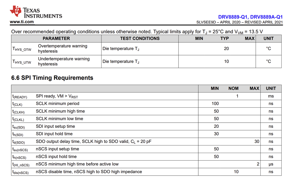
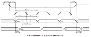
It is necessary to ensure that t(READY), t(HI_nSCS), tdis(nSCS) are within the specifications.
Do you have any suggestion how to conduct this test?

Thanks & best regards,

  • Hi David,

    We have validated the specifications already and published these in the datasheet. I don't think there is a easy way to measure these parameters precisely. For example for t(READY) t0 must start as soon as VM > VRST and start doing SPI reads until you get a successful read out of a known register default value. Likewise for t(HI_nSCS) you must perform back to back SPI transactions and find at what nSCS high time the transaction fails. I have never seen any customer do this verification. Please let us know if there is a specific issue or concern that prompted this verification need. Thanks.

    Regards, Murugavel

  • Hi Murugavel, 

    1.

    We have validated the specifications already and published these in the datasheet.

    I would like to know which page that mention regarding this matter? 

    2.

    VM > VRST

    In datasheet it state Nom at 1ms, so if the result is more than 1ms is it possible and the result is it okay? 

    3.

    t(HI_nSCS) you must perform back to back SPI transactions and find at what nSCS high time the transaction fails.

    How can i do this kind of test as an Test Engineer? it would be really helpful if you can provide the picture 

    4. 

    I have never seen any customer do this verification. Please let us know if there is a specific issue or concern that prompted this verification need.

    Same here! It's new for us too. This is part of our new design verification for I2C, so please help us fix this issue.

    Thank you, Via

  • Hi Via,

    1. Please see below. There is a typo in one of the specifications t(HI_nSCS), it is the MIN value not the MAX value.  

    2. "VM > VRST, In datasheet it state Nom at 1ms, so if the result is more than 1ms is it possible and the result is it okay? ". Yes it is fine. Any time > 1ms.

    3. I'm not familiar with testers. I'm not sure how you can do this with a tester. t(HI_nSCS) is already specified in the datasheet. Any value > MIN parameter is okay to use in the application.

    4. You said "This is part of our new design verification for I2C". The DRV8889-Q1 does not have I2C. It is an SPI interface. All our testing performed are TI proprietary. You can establish a test protocol based on the device datasheet which is he public information we have for this device.

    If you have specific questions on the SPI we can answer. As you may have notice the MIN specification is the fastest that can be supported by the device for SPI under the recommended operating conditions of the device. Any timing higher than the MIN value or NOM value are guaranteed to work with no issues. 

    Thank you.  

  • Hi Murugavel, 

    1.

    Please see below. There is a typo in one of the specifications t(HI_nSCS), it is the MIN value not the MAX value. 

    Thank you for the confirmation!

    2.

    "VM > VRST, In datasheet it state Nom at 1ms, so if the result is more than 1ms is it possible and the result is it okay? ". Yes it is fine. Any time > 1ms.

    Got it!

    3. 

    I'm not familiar with testers. I'm not sure how you can do this with a tester. t(HI_nSCS) is already specified in the datasheet. Any value > MIN parameter is okay to use in the application.

    Okay got it! I'll do according to your suggestion 

    4. 

    It is an SPI interface.

    Oh I'm Sorry my mistake, i mean for timing measurement. because In the previous case, a communication anomaly occurred during testing. It is now necessary to add timing measurements during test to confirm compliance with specifications. 

    During design review, timing needs to be determined based on specifications. That's why we need to know more about this

    Thank you, 

    Via

  • Hi Via,

    Thank you. Hopefully my inputs were helpful. Kindly either David or yourself close this thread at your end.

    Regards, Murugavel

  • Hi Murugavel, 

    Sorry, i have one more question. this one still relate . 

    t(READY) t0 must start as soon as VM > VRST and start doing SPI reads until you get a successful read out of a known register default value.

    In the SPI datasheet, it states >1ms, but on the other hand, it states a maximum of 0.9ms. So, which one is correct?

    and it's hard for us to imagine this situation, because when we check this there is no information regarding t(READY)

  • Oh and one more, 

    Which one is the VRST Pin?

    is it DRV_off is the VRST Pin ?

    Thank you,

    Via

  • Hi Via,

    The 0.9ms MAX is from VM > UVLO whereas the 1ms NOM is from VM > VRST. I'd consider the "time it takes from VM > UVLO here 4.45V + 0.9ms" which may amount to 1ms or little over 1ms depending on your power supply voltage ramp up time. 

    VRST is VM voltage for reset. It is a VM voltage level not a pin.

    Regards, Murugavel

  • Hi Murugavel, 

    So how do i test it then ? 

    should i compare it with VIN and CS to check the time ? 

    Thank You, 

    Via

  • Hi Via,

    CS (nSCS) is an external input to the DRV8889-Q1. You cannot use that to check the time. You may have perform an SPI write and read of a writable register, for example CTRL1, 2 or 3 with a known value and compare to see if the read back matched the written value. This has to be done fast enough to find out the time it takes to get a valid read after a write. 

    Regards, Murugavel

  • Hi Murugavel, 

    So it can only be test by Software i assume ? 

    because it's not in my expertise, let me discuss it with our Software engineer and let you know 

    Thank you

    Via