This thread has been locked.

If you have a related question, please click the "Ask a related question" button in the top right corner. The newly created question will be automatically linked to this question.

DRV8256: Review of circuit and overall suitability for use (DRV8256ERGER)

Part Number: DRV8256


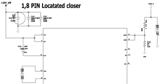
We are considering using TI's Motor Drive IC (DRV8256ERGER).
We would like to ask you to review the circuit configuration and overall suitability for use.

If there are any other considerations other than the three below, please mention them.
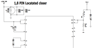
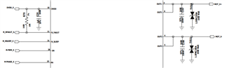
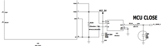
1. Circuit review


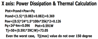
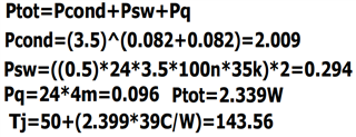
2. Suitable of Tj calculation (inner MOSFET)

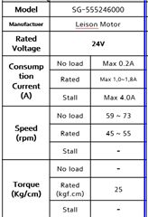
3. Review of Motor Specification (Suitable to use this motor drive IC)

  • Hi In Suk,

    I will review this and provide you a feedback by tomorrow Dallas time. Thanks.

    Regards, Murugavel

  • Hi In Suk,

    1. Circuit review, C160 must be sized according to motor inrush current requirement and the total capacitance available in the power supply and the length of the connection between power supply and the +24V_VM.

    For DVDD, it is recommended to connect a X7R, 0.47- μF to 1-μF, 6.3-V or 10-V rated ceramic capacitor to GND. DVDD is an internal regulator output intended for internal use of the device and it must not be externally loaded. In the schematic where is DVDD_R connected? 

    C167 and 168, 100nF may cause additional drive losses if used with PWM input for example 20kHz. In this case a lower value capacitor is recommended. You can use a 100nF capacitor across motor terminals usually provided close to the motor.

    The nFAULT pin requires a pullup resistor, it is a open drain output. Please refer to the datasheet.

    The input is showing PH/EN control. I noticed you mentioned DRV8256ERGER which is the correct version for PH/EN control.

    There's an external current sense resistor and amplifier for MCU analog input. Is this for monitoring current? Are you also using internal current regulation. I see you have provided VREF input. 

    2. I noticed you calculated Tj for Ta = 50C which is a high ambient temperature. The estimated value of 143.56C is pretty close to the OTSD MIN spec in the datasheet. How long this level of dissipation will last? The margin is pretty low. There is a risk of  OTSD happening in your circuit under the calculated operating conditions. 

    3. The stall current max. is specified to be 4A for this motor. The driver IOCP MIN spec is 8A which has a good margin. This driver is suitable for use with this motor from this standpoint.

    Thank you.

    Regards, Murugavel

  • I will reply your comment at each number.

    1.

    1) The capacitance size applied to the VM is not only the size shown in the picture, but also 330uF (Elec capacitor).

    +24_VM is the power supply after passing the Filter at +24V. Therefore, the capacitance value of the VM of the Motor Drive IC is 340.2uF (300+10+0.1+0.1).

    2) I added an additional 1uF capacitor. DVDD_R is used to connect to Pin12, 13 (VREF). (You can see it in the picture)

    3) OUT1(Pin3,6) and OUT2(Pin4,5) are output pins that go out from the Drive IC. The orientation in the picture is incorrect.

    Would it be better to place C167 and C168 closer to the IC? Would it be better to place it behind the TVS diode, i.e. at the output?

    4) The fault-related pin is pulled-up connected.

    5) External current sense resistor and amplifier for MCU analog input is monitoring current value. Also using internal current regulation.

       Power for current sense IC used VCC_5V . This is external 5V.

    2. In the calculated formula, the current value is reflected close to the stall current value. The current value that actually flows is rated at around 1.5A, as specified in the Motor Specification. If calculated at 1.5A, the Tj value will be up to 73 degrees. In reality, the high current of 3.5A is only exposed to the motor for a very short time during initial operation.

    If the situation is similar to the one described above, the margin is expected to be high. What is Murugavel's opinion?

    3. No comment.

  • Hi In Suk,

    Thanks for the update.

    1. Understood. That should be good for bulk capacitance.

    2. Yes, looks fine.

    3.  "Would it be better to place C167 and C168 closer to the IC? Would it be better to place it behind the TVS diode, i.e. at the output?". At the output connector would be better.

    4. I see it. Note that nFAULT is pulled up to DVDD which is 5V TYP. I assume the input logic of the controller you use supports 5V logic levels. 

    5. Thanks for the clarification. This is fine. DVDDX is a low current LDO. This is why we're recommending to not use external loads other than VREF and pullup. 

    "In the calculated formula, the current value is reflected close to the stall current value. The current value that actually flows is rated at around 1.5A, as specified in the Motor Specification. If calculated at 1.5A, the Tj value will be up to 73 degrees. In reality, the high current of 3.5A is only exposed to the motor for a very short time during initial operation.

    If the situation is similar to the one described above, the margin is expected to be high. What is Murugavel's opinion?". I think this should be fine. 

    Regards, Murugavel