Hi,
In DRV8353H, I have two queries:
Query 1:
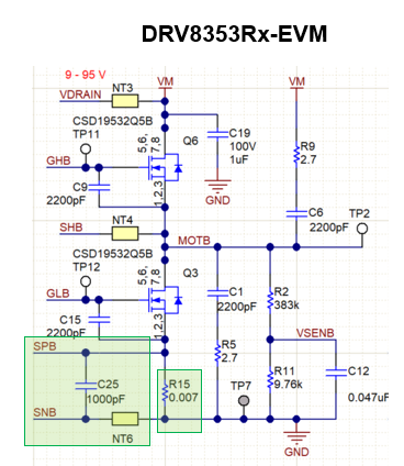
SPA,SPB,SPC pins are common for bottom phase gate current return path and Current sensing input to the driver for the respective phases of A,B,C. if i have to add filter after shunt sensing(i.e Filter at input of Gate driver current amplifiers), Could you please suggest a scheme for this ? I could see that, if i add filter, it will break the Current path bottom FET gate current.
Query2:
In data sheet, Charge pump current limit current reduces as VM voltage reduces as shown in yellow highlighted below. Does it mean that if i use at VM =10V, Only 15mA(Instead of Max 25mA) is the limit so that MOSFET selection to be there accordingly. Then, why did the absolute Max says 25mA is the limit ?

-
Ask a related question
What is a related question?A related question is a question created from another question. When the related question is created, it will be automatically linked to the original question.