This thread has been locked.

If you have a related question, please click the "Ask a related question" button in the top right corner. The newly created question will be automatically linked to this question.

DRV8908-Q1: How to configure DRV8908 used as high side switch in digital output application?

Part Number: DRV8908-Q1

Hi team, 

We just fanout in DRV8908 in PLC as digital output application. When they applied the driver as high side applications, following the reference timing, there is no signal on the output.

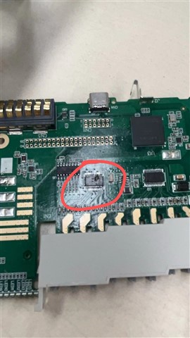
They formerly used MPQ6527 in mass production projects, and do early evaluation by placing MPQ6527 of DRV8908 on the red rectangle area. Only changed DRV8908 FAULT pin floating. The attached schematic of MPQ6527 is showed below. 

Support need: 

  1. Can you please help check if drop in evaluation on MPQ6527 is OK by only changing Fault pin floating? 

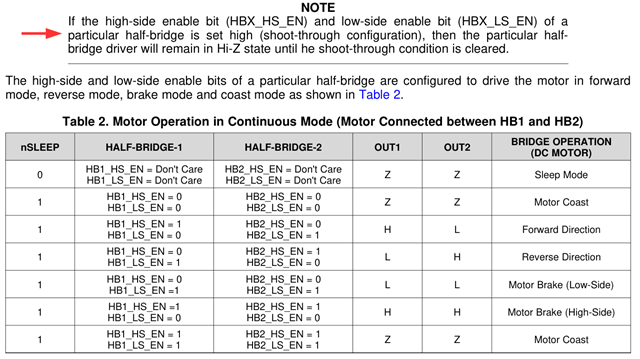
  1. From reading software configuration in below, the SPI timing is set to 1.25MHz. But there is no output signal since no led indication is lighting on.


Write Config Ctrl register parameter: 0x0706
Write OP Ctrl_1 register parameter: 0x08AA
Write OP Ctrl_2 register parameter: 0x09AA
Read IC_STAT register parameters: 0x4000
The VM is from 24V external which means external power supply is 24V, so one bit in the first round of configuration 0x0706 is to change the default overvoltage detection level from 21V to 33V. After reading the status register, it was determined that there was an overvoltage exception, and a round of reconfiguration was performed. The write configuration register was changed to 0x0707, clearing the previous status register information.

Can you help to check on how to perform normal output and configure right register on this case? Thank you!

  • Hey Zoe,

    Looks like the pin configuration should work.

    The VM is from 24V external which means external power supply is 24V, so one bit in the first round of configuration 0x0706 is to change the default overvoltage detection level from 21V to 33V. After reading the status register, it was determined that there was an overvoltage exception, and a round of reconfiguration was performed. The write configuration register was changed to 0x0707, clearing the previous status register information.

    From this it sounds like SPI communication is working, so that's good! Make sure they are following the SPI timing requirements:

    Is the Enable pin High?

    See 8.3.1.1 Control Modes  and make sure settings described there are followed. 

    Regards,

    Jacob

  • Hi Jacob,

    Abnormal burning scenario occurred when put DRV8908 on their digital output module. Thermal pad and pin17/18 were connected to the ground.

    The burned position is always on PIN17/18.When connect VM to 24V, it directly burned out.

    In the first place, the output is normally working. once connected with 1.9A electric load, the whole 24V shut down and IC burned out on the same position.

    Can you help check what cause this issue when directly drop in on MPS MPQ6527 layout? This will help we faster compete with MPS in mature mass production platfom.


  • Hey Zoe,

    We have seen some odd behavior when using electronic loads.  Do you happen to have some power resistors to do the testing?  Such as a 32Ω resistor or similar.  If using the E-Load try to take a scope capture of the load turning on, make sure that its slew rate is slow enough that it does not exceed device limits during blanking time.  

    Double check the board for no solder shorts, since this is unconventional board assembly.  

    Best,

    Jacob

  • Customer feedback they turned E-Load by 100mA per time. MPS part number is MPQ6527. What's next step for debug the burn out?

  • Does this occur when the ELoad gets to 1.9A?  This device OCP limit is 1.8A typical (1.3A min / 2.3A max), so 1.9A should trip OCP and cause the outputs to turn off.  We are not sure what the E-Load does when the load is instantly removed - this might be causing a voltage spike.  If you got up to 1.9A with the E-Load I suspect this is what is burning the device. Overvoltage events are what cause most of device damage like this. 

    Please try it with a physical load, not the E-Load.  Power resistor or motor good. 

    Can you show on the PCB where the bulk capacitor is, and are the VM decoupling capacitors (0.01uF for this device) located near the VM pins? 

    Are there multiple DRV devices on the board, with different behaviors between them?  

    I compared the Land Pattern of the two devices, and they do match up perfectly, so that's good.  Still be observant for solder shorts.  

    Can you explain what the expected load for this is?  PLC is important market we are trying to improve on, and understanding the expected load to be connected to the output is valuable.   Will it be a valve, a motor, a light, etc? 

    Regards,

    Jacob