This thread has been locked.

If you have a related question, please click the "Ask a related question" button in the top right corner. The newly created question will be automatically linked to this question.

DRV8714-Q1: Requirements for waveforms that can be applied to Vinx

Part Number: DRV8714-Q1

Tool/software:

Hi team.

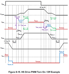
What are the requirements for waveforms that can be applied to Vinx?
As far as I can see from the diagram below, I believe that if Vinx does not output Hi for at least the following total time, the upstream or downstream FET will be half-ON.
"tPD"+"Fall time of VGSLx"+"tDEAD"+"tDON"+"Rise time of VSHx from VSHx_L to VSHx_H"+"tPST_CHR"

Do you agree with the above idea?
Also, in that case, where is the "tPD" time defined?

  • Hi,

    Thank you for your question. May 27th Monday is national holiday in US. Will feedback to expert back office

  • Hi,

    Thank you for your questions.

    VINX on top is representative of input signal from MCU. It could be PWM signal normally comes to INx pin from MCU.

    tPD is propagation delay from above logic input to output start reacting. Can be considered as internal (digital) signal propagation delay.

    >>Do you agree with the above idea?

    Unfortunately, I do not understand your question. However, above my response solve your question.

    regards

    Shinya Morita

  • Morita-san

    Thankyou for your response.
    But my question is not solved.

    If a very low duty is applied to Vinx, I think the output will turn off before Vgshx reaches Hi.
    I would like to calculate how much duty is needed to make Vgshx reach Hi.

    Could you please tell me how to calculate this?

  • Hi ,

    Thank you for your questions

    >>If a very low duty is applied to Vinx, I think the output will turn off before Vgshx reaches Hi.

    Yes, this is correct.

    >>I would like to calculate how much duty is needed to make Vgshx reach Hi

    This is determined by customer's application like external FET, DRV's register setting of IDRIVE etc. Rise and fall time of output is not determined by DRV's performance.

    Based on above background, here is example. 

    I customer's OUTPUT rise and fall time are 5us and PWM frequency is 20KHz(50us), 5usec is 10% of 20KHz.

    Customer will not have good output pulse while MCU's PWM is 0-10% and 90-100%.

    regards

    Shinya Morita