


Tool/software:
Hi,
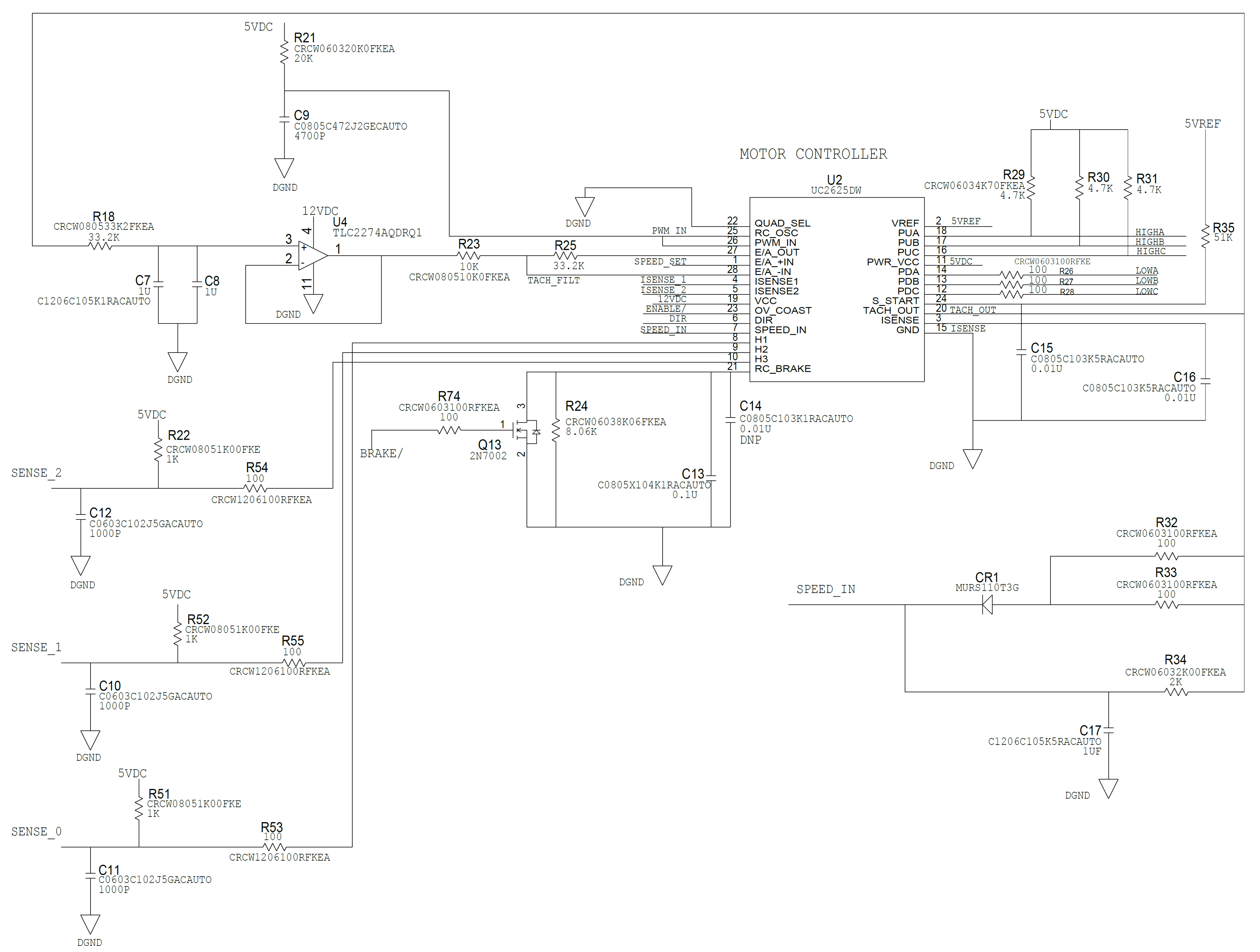
we are using UC2625MDWREP chip in one of our product.
Problem Statement:
The motor is not running at the intended RPM as per design due to the U2 chip (UC2625MDWREP) leads to product ATP failure.
Problem Description:
The design was completed & the issue is 40% of the boards are working fine as expected and remaining boards failure at RPM level i.e. The RPM is lower from the intended level.
Based on the root cause analysis the inputs to the UC2625MDWREP was maintained in the same level in both Passed and Failed boards. The passive components used with UC2625-EP were 1% tolerance and the component level similarity checks were completed between working & Non-working boards.
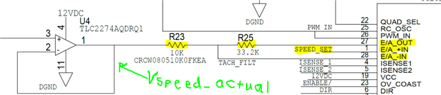
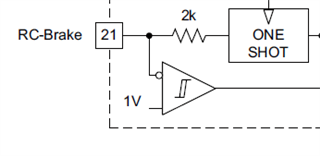
On further analysis, the signal level checks were performed and the signal level difference was found onto the UC2625-EP input and outputs even though the input control signal is same. The signal which are monitored are E/A_OUT (Pin 27), PWM IN (Pin 26), RC BRAKE (Pin 21) & PDC (Pin 12). During the waveform capture process the E/A_IN+ was maintained constant with a external precision DC source of 2.260 VDC for both working & non-working boards.
Note:-
Channel 1: RC BRAKE (Pin 21)
Channel 2: PWM IN (Pin 26)
Channel 3: EA_OUT (Pin 27)
Channel 4: PDC (Pin 12)
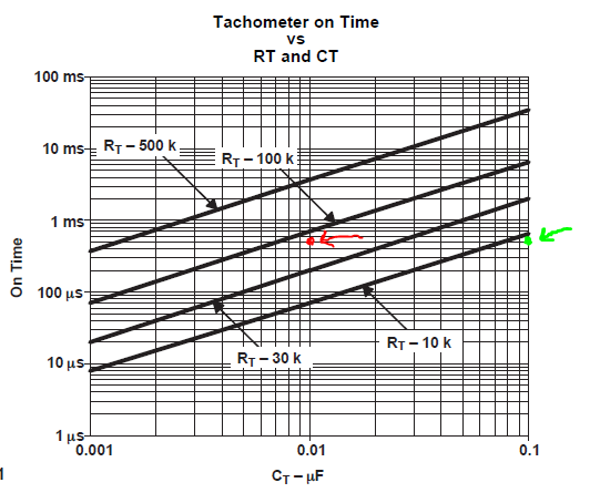
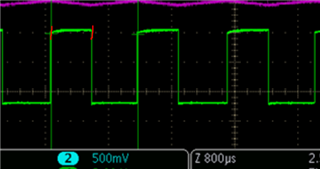
As the snippet cursor shows there is a commutation cycle difference is more than 100uS and it is uniform in all failed boards.
Working board: PWM pulse @ PDC (Pin 12) ON time - 28.6 uS OFF time - 17 uS
Non-working board: PWM pulse @ PDC (Pin 12) ON time - 27.2 uS OFF time - 18 uS
Kindly explain why this difference is seen from the chip to chip in terms of commutation cycle, PWM ON & OFF time?
To add more information the chip with device marking 34Z01GV was failing at 60% rate whereas 98Z05GV chips are pass at 100%. The attached waveforms also comparison between 34Z01GV (non-working) & 98Z05GV (working) Boards.
Also clarify the difference of 34Z01GV & 98Z05GV batch chip.
The error amplifier inputs and output are monitored for the same boards and seen 50mV difference on the same. why the IC EA_OUT are not settling at same voltage for the given same speed command. waveforms for the same attached below.
Note:-
Channel 1: EA IN+ (Pin 1)
Channel 2: EA IN- (Pin 28)
Channel 3: NC
Channel 4: EA OUT (Pin 27)
why the different batch ICs generates a 50mV different settling voltage band at EA OUT (Pin 27) for the same inputs?.
Regards,
Booshan S


