This thread has been locked.

If you have a related question, please click the "Ask a related question" button in the top right corner. The newly created question will be automatically linked to this question.

DRV2667: No boost power

Part Number: DRV2667

Tool/software:

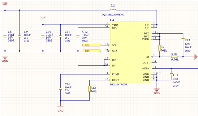
I have trouble getting the boost converter running on the DRV2667.

What I have verified, is:

* The I2C interface is working (reading/writing registers and memory)
* Vreg = 1.8V is ok.
* Vpump = 7.6V should be ok (the datasheet does not specify this voltage).
* Vrext = 1.3V is ok.
* Vbst = Vin = 5.8V
* Using a scope, no switching action is observed on the SW, BST or PVDD nodes.

The powerup sequence as been followed (Reset => Out of standby => Setup => Writing FIFO).

Reading back the registers, the status/config is:
0x00: Status = 0x00
0x01: Config = 0x3a = 111010b: Digital input + Gain 2.
0x02: Config = 0x0e = 1110b: Timeout 3 + EN_OVERRIDE

Data is being written 16 bytes at a time, no delay in between.
The I2C frequency is 40 kHz.
  • Hello,

    Thanks for reaching out. I am doing a schematic review first and will get back to you this afternoon. 

    Regards,
    Sydney Northcutt

  • Update:

    Strapping L2 to the 3.3V supply, the switcher will start. Apparently, it matters to the chip if the switch node is equal to VDD before activating. Maybe it a precaution to not start switching into a "hot" BST node?

    Also, with large REXT resistors, the boost supply fails to start. It looks like I have to reduce REXT to about 15k (Current limit at 0.941A) to get 100V output.
    I think this indicate a quiescent current draw of about 16mA on PVDD. This is much, as the datasheet specify 130 uA for digital modes.

  • Hi Ivar,

    Yes, L2 should be tied to VDD. 5.8 V is out of the recommended spec for the device. 

    The Rext resistor should be between 6kΩ and 35 kΩ, so changing it to 15 kΩ is okay. The previous value was too high. You are also correct that the current limit is now 0.941 A, but that is the current limit that will be pulled through the power supply. That being said, the saturation current of your inductor (L2) needs to be rated higher than the programmed current limit. The limit is 0.941 A, but your inductor saturation current is rated for 30 mA. I think this is your main issue here. I recommend swapping to an inductor with a saturation current of at least 1 A. 

    Regards,
    Sydney Northcutt 

  • I have requested new parts, and will try them as they arrive this week.

    The SW pins is the boost switching node. During normal operations, that voltage bounce between 0V and Vbst, approximately.
    As such, 5.8V is not really out of range for this pin, and I think its strange that I cannot switch from a higher voltage than VDD.

    The reason being efficiency in the PDN. If the chip really draws 16-20 mA quiescent current from PVDD running idle, I need to deliver 20*(100-3.3)/3.3 = 586 mA static current through the 3.3V supply. If instead I could switch off the 5.8V supply, or even my 24V systems supply, the PDN current would be greatly reduced. 

  • Hi Ivar, 

    5.5 V is the recommended max for VDD. The voltage applied to the boost inductor should be tied to or equal VDD. Essentially this is due to the comparators inside the device This thread has more information: link. You are correct though that the SW pin will be switching from 0V to around Vbst. For more information on the boost design of this device, we have this app note

    Regards,
    Sydney Northcutt

  • The link points to a page that cannot be find. It seems like an internal forum that I cannot access?

    It may be related to this case: (1) DRV2665: DRV2665/DRV2667 External Boost - Motor drivers forum - Motor drivers - TI E2E support forums

    Anyway, I have received information to proceed with my design.