Other Parts Discussed in Thread: TINA-TI
Tool/software:
Hello all,
I would like to import this attached .lib into my simscape electrical.This is my code:
*$
* LM5122
*****************************************************************************
* (C) Copyright 2020 Texas Instruments Incorporated. All rights reserved.
*****************************************************************************
** This model is designed as an aid for customers of Texas Instruments.
** TI and its licensors and suppliers make no warranties, either expressed
** or implied, with respect to this model, including the warranties of
** merchantability or fitness for a particular purpose.  The model is
** provided solely on an "as is" basis.  The entire risk as to its quality
** and performance is with the customer
*****************************************************************************
*
* This model is subject to change without notice. Texas Instruments
* Incorporated is not responsible for updating this model.
*
*****************************************************************************
*
** Released by: Texas Instruments Inc.
* Part: LM5122
* Date: 03JAN2020
* Model Type: TRANSIENT
* Simulator: PSPICE
* Simulator Version: 16.2.0.p001
* EVM Order Number: LM5122EVM-1PH
* EVM Users Guide: SNVU197 JANUARY 2013
* Datasheet: SNVS954D-APRIL 2013-REVISED SEPTEMBER 2013
* Topologies Supported: Boost
*
* Model Version: Final 1.20
*
*****************************************************************************
*
* Updates:
*
* Final 1.20
* .END statement is removed from LINE 745
*
* Final 1.10
* Bugfix.
*
* Final 1.00
* Release to Web.
*
****************************************************************************
.SUBCKT LM5122_TRANS SLOPE RES FB HO LO SS SW PGND MODE AGND BST
+  COMP SYNC_OUT SYNC_RT_IN CSN CSP VCC VIN UVLO OPT EP
RDAP EP 0 1m
X_U7_U11         U7_N16771766 DIODE_EM MODE_OFF AND2_BASIC_GEN PARAMS: VDD=1
+  VSS=0 VTHRESH=500E-3
X_U7_U1         U7_N16771736 COMP_OFF U7_N16771766 COMP_BASIC_GEN PARAMS: VDD=1
+  VSS=0 VTHRESH=0.5
E_U7_ABM1         U7_N16771736 0 VALUE { V(MODE) - 20m + 40m*V(MODE_OFF)    }
R_U7_R16         MODE U7_N00072  700k TC=0,0
R_U7_R21         0 MODE  100k TC=0,0
V_U7_V2         U7_N00072 0 1.2
X_U7_U2         U7_N16772381 MODE DIODE_EM COMP_BASIC_GEN PARAMS: VDD=1 VSS=0
+  VTHRESH=0.5
V_U7_V1         U7_N16772381 0 1.24
R_R2         0 OPT  1G TC=0,0
V_U4_V1         U4_N16777456 U4_N16777502 0.4
X_U4_U6         U4_N16777451 SHUTDOWN BUF_BASIC_GEN PARAMS: VDD=1 VSS=0
+  VTHRESH=0.5
X_U4_U7         U4_N16777425 STANDBY_N BUF_BASIC_GEN PARAMS: VDD=1 VSS=0
+  VTHRESH=0.5
E_U4_E1         U4_N16777502 0 SHUTDOWN_N 0 -0.1
V_U4_V3         U4_N16778460 0 5
X_U4_U2         U4_N16777456 UVLO U4_N16777445 COMP_BASIC_GEN PARAMS: VDD=1
+  VSS=0 VTHRESH=0.5
V_U4_V2         U4_N16777550 0 1.2
X_U4_U3         STANDBY_N STANDBY INV_BASIC_GEN PARAMS: VDD=1 VSS=0
+  VTHRESH=500E-3
X_U4_U4         SHUTDOWN SHUTDOWN_N INV_BASIC_GEN PARAMS: VDD=1 VSS=0
+  VTHRESH=500E-3
X_U4_D28         UVLO U4_N16778460 d_d1 PARAMS:
G_U4_G1         0 UVLO U4_N16777423 0 10u
X_U4_U1         UVLO U4_N16777550 U4_N16777423 COMP_BASIC_GEN PARAMS: VDD=1
+  VSS=0 VTHRESH=0.5
R_U4_R1         U4_N16777423 U4_N16777425  721.5 TC=0,0
C_U4_C1         0 U4_N16777425  10n
R_U4_R2         U4_N16777445 U4_N16777451  721.5 TC=0,0
C_U4_C2         0 U4_N16777451  10n
X_U8_U17         U8_15U_ON U8_CH one_shot PARAMS:  T=10
X_U8_S6    U8_N80792 0 RES 0 HICCUP_U8_S6
G_U8_G1         0 RES U8_N70829 0 35u
X_U8_U30         U8_N90156 U8_N90374 U8_N90442 COMP_BASIC_GEN PARAMS: VDD=1
+  VSS=0 VTHRESH=0.5
R_U8_R1         0 HICCUP  1k TC=0,0
V_U8_V11         U8_N89978 0
+PULSE 1 0 10n 1n 1n 10000 100000.1
X_U8_U618         U8_HICCUP_N EN30 U8_N70829 AND2_BASIC_GEN PARAMS: VDD=1 VSS=0
+  VTHRESH=500E-3
X_U8_U609         U8_N90436 U8_N89978 U8_HICCUP_DONE OR2_BASIC_GEN PARAMS:
+  VDD=1 VSS=0 VTHRESH=500E-3
X_U8_U8         U8_N74555 RES U8_RES_2V COMP_BASIC_GEN PARAMS: VDD=1 VSS=0
+  VTHRESH=0.5
X_U8_U20         U8_N94079 EA_DIS U8_5U_ON N94329 SRLATCHRHP_BASIC_GEN PARAMS:
+  VDD=1 VSS=0 VTHRESH=0.5
X_U8_U19         U8_RES_2V U8_RES_4V U8_15U_ON N90088 SRLATCHRHP_BASIC_GEN
+  PARAMS: VDD=1 VSS=0 VTHRESH=0.5
X_U8_U7         RES U8_N74376 U8_RES_4V COMP_BASIC_GEN PARAMS: VDD=1 VSS=0
+  VTHRESH=0.5
V_U8_V2         U8_N74376 0 4
G_U8_G3         RES 0 U8_5U_ON 0 5u
X_U8_U37         U8_N90442 U8_N90436 one_shot PARAMS:  T=120
X_U8_D11         0 U8_N90156 d_d PARAMS:
V_U8_V1         U8_N72039 0 1.2
X_U8_U610         HICCUP U8_N96722 U8_15U_ON U8_N73798 AND3_BASIC_GEN PARAMS:
+  VDD=1 VSS=0 VTHRESH=500E-3
X_U8_U611         SHUTDOWN U8_HICCUP_DONE U8_N80792 OR2_BASIC_GEN PARAMS: VDD=1
+  VSS=0 VTHRESH=500E-3
X_U8_D1         0 RES d_d PARAMS:
C_U8_C11         0 U8_N90156  10n  TC=0,0
X_U8_U10         EA_DIS U8_N96722 INV_BASIC_GEN PARAMS: VDD=1 VSS=0
+  VTHRESH=500E-3
X_U8_S5    U8_HICCUP_N 0 U8_N90156 0 HICCUP_U8_S5
V_U8_V3         U8_N74555 0 2
X_U8_U6         RES U8_N72039 U8_N72262 COMP_BASIC_GEN PARAMS: VDD=1 VSS=0
+  VTHRESH=0.5
V_U8_V10         U8_N90374 0 7.5
X_U8_U18         U8_N72262 U8_HICCUP_DONE HICCUP U8_HICCUP_N
+  SRLATCHRHP_BASIC_GEN PARAMS: VDD=1 VSS=0 VTHRESH=0.5
V_U8_V12         U8_N94079 0
+PULSE 1 0 10n 1n 1n 10000 100000.1
G_U8_ABMII5         0 U8_N90156 VALUE { V(U8_CH)    }
G_U8_G2         0 RES U8_N73798 0 15u
R_R1         0 OPT  1G TC=0,0
E_U2_E2         U2_CSP_CSN 0 CSP CSN 1
X_U2_U6         U2_N16811606 U2_N16814522 U2_CL COMP_BASIC_GEN PARAMS: VDD=1
+  VSS=0 VTHRESH=0.5
X_U2_U608         U2_PWM_PRE U2_N16935498 INV_DELAY_BASIC_GEN PARAMS: VDD=1
+  VSS=0 VTHRESH=0.5 DELAY=15n
X_U2_U19         U2_N16971049 U2_N17026282 U2_N16968265 N16970506
+  SRLATCHRHP_BASIC_GEN PARAMS: VDD=1 VSS=0 VTHRESH=0.5
X_U2_D28         U2_N16935544 U2_MIN_ON d_d1 PARAMS:
G_U2_ABMI1         U2_MIN_ON U2_N16935544 VALUE {
+  10p*0.5/(0.8*V(RSLOPE_NORM)+410n)    }
X_U2_U609         U2_PWM_PRE U2_MIN_ON U2_N16935582 OR2_BASIC_GEN PARAMS: VDD=1
+  VSS=0 VTHRESH=500E-3
X_U2_U625         STANDBY_N U2_HICCUP_N U2_HO_LO_OFF AND2_BASIC_GEN PARAMS:
+  VDD=1 VSS=0 VTHRESH=500E-3
X_U2_S1    U2_EA_DIS_N 0 U2_N16923893 COMP PWM_U2_S1
X_U2_U10         U2_PWM U2_N16861216 INV_BASIC_GEN PARAMS: VDD=1 VSS=0
+  VTHRESH=500E-3
X_U2_U613         U2_PWM_OUT MAX_ON_TIME U2_N16945781 OR2_BASIC_GEN PARAMS:
+  VDD=1 VSS=0 VTHRESH=500E-3
V_U2_V4         U2_N16971725 0 7m
X_U2_U12         HICCUP U2_HICCUP_N INV_BASIC_GEN PARAMS: VDD=1 VSS=0
+  VTHRESH=500E-3
X_U2_U611         U2_N16919029 U2_CL U2_OCL AND2_BASIC_GEN PARAMS: VDD=1 VSS=0
+  VTHRESH=500E-3
X_U2_U17         EA_DIS U2_EA_DIS_N INV_BASIC_GEN PARAMS: VDD=1 VSS=0
+  VTHRESH=500E-3
X_U2_U626         U2_RST MODE_OFF U2_N16994005 OR2_BASIC_GEN PARAMS: VDD=1
+  VSS=0 VTHRESH=500E-3
X_U2_U621         U2_CSP_CSN U2_N16971725 U2_N17026282 COMP_BASIC_GEN PARAMS:
+  VDD=1 VSS=0 VTHRESH=0.5
V_U2_V2         U2_N16814522 0 750m
X_U2_U612         U2_CL U2_N16919029 INV_DELAY_BASIC_GEN PARAMS: VDD=1 VSS=0
+  VTHRESH=0.5 DELAY=25n
X_U2_U610         U2_HO_LO_OFF U2_N16861216 U2_N16861605 PWMH AND3_BASIC_GEN
+  PARAMS: VDD=1 VSS=0 VTHRESH=500E-3
V_U2_V5         U2_N16973766 0 5m
X_U2_U622         U2_N16973766 U2_CSP_CSN U2_N16971049 COMP_BASIC_GEN PARAMS:
+  VDD=1 VSS=0 VTHRESH=0.5
G_U2_G2         CSN 0 STANDBY_N 0 10u
E_U2_SUM1         U2_N16771383 0 VALUE {V(RAMP_SL)+V(U2_N16811606)}
X_U2_U615         U2_HO_OFF U2_HO_OFF U2_N16861605 OR2_BASIC_GEN PARAMS: VDD=1
+  VSS=0 VTHRESH=500E-3
X_U2_U15         U2_N16896652 U2_N16935582 U2_PWM AND2_BASIC_GEN PARAMS: VDD=1
+  VSS=0 VTHRESH=500E-3
C_U2_UPWM2_C25         0 U2_UPWM2_N00254  10n  TC=0,0
R_U2_UPWM2_R29         U2_UPWM2_N00234 U2_UPWM2_N00254  1000 TC=0,0
E_U2_UPWM2_E3         U2_UPWM2_N00306 0 U2_UPWM2_N00254 0 1
E_U2_UPWM2_ABM2         U2_N16923893 0 VALUE {
+  LIMIT(V(U2_UPWM2_N00306),-0.02,V(U2_UPWM2_EA_CLAMP))     }
E_U2_UPWM2_ABM3         U2_UPWM2_EA_CLAMP 0 VALUE { IF(V(VIN) < 5.5, 3, 3.3)
+  }
E_U2_UPWM2_E2         U2_UPWM2_N00234 0 REF FB 10K
E_U2_E1         U2_N16811606 0 CSP CSN 10
X_U2_U18         U2_N16945781 U2_OCL EN05 EN30 SRLATCHRHP_BASIC_GEN PARAMS:
+  VDD=1 VSS=0 VTHRESH=0.5
X_U2_U5         U2_N16771383 COMP_OFF U2_PWM_OUT COMP_BASIC_GEN PARAMS: VDD=1
+  VSS=0 VTHRESH=0.5
X_U2_U16         CLK U2_N16994005 U2_PWM_PRE N16995360 SRLATCHRHP_BASIC_GEN
+  PARAMS: VDD=1 VSS=0 VTHRESH=0.5
X_U2_U607         U2_N16935498 U2_PWM_PRE U2_N16935544 AND2_BASIC_GEN PARAMS:
+  VDD=1 VSS=0 VTHRESH=500E-3
G_U2_G1         CSP 0 STANDBY_N 0 11u
V_U2_V3         U2_N16896652 0 1
C_U2_C140         0 U2_MIN_ON  10p
E_U2_ABM1         REF 0 VALUE { min(V(SS_INT), 1.2)    }
X_U2_U11         U2_HO_LO_OFF U2_PWM PWML AND2_BASIC_GEN PARAMS: VDD=1 VSS=0
+  VTHRESH=500E-3
V_U2_V7         COMP COMP_OFF 1.1
X_U2_U620         MAX_ON_TIME U2_CL U2_PWM_OUT U2_RST OR3_BASIC_GEN PARAMS:
+  VDD=1 VSS=0 VTHRESH=500E-3
X_U2_U624         U2_N16968265 DIODE_EM U2_HO_OFF NAND2_BASIC_GEN PARAMS: VDD=1
+  VSS=0 VTHRESH=500E-3
C_U6_C1         0 RAMP_SL  10n  TC=0,0
X_U6_U14         0 U6_N16811121 CLK U6_N16836630 OR3_BASIC_GEN PARAMS: VDD=1
+  VSS=0 VTHRESH=500E-3
X_U6_S2    U6_N16836630 0 RAMP_SL 0 Slope_Generator_U6_S2
G_U6_ABMII3         U6_N16833608 U6_TS VALUE { V(U6_N16833710) * 1    }
X_U6_U23         U6_N16833710 U6_N16864716 INV_BASIC_GEN PARAMS: VDD=1 VSS=0
+  VTHRESH=500E-3
C_U6_C5         0 U6_TS  1  TC=0,0
E_U6_ABM3         U6_MAX_OFF_TIME 0 VALUE { IF(V(VCC) < 5.5, 560n, 330n)    }
X_U6_U25         U6_N16864718 SHUTDOWN U6_CNTR_DISABLE U6_N16863310
+  SRLATCHRHP_BASIC_GEN PARAMS: VDD=1 VSS=0 VTHRESH=0.5
E_U6_E2         RSLOPE_NORM 0 SLOPE 0 1p
V_U6_V7         U6_N16881517 0 1.2
X_U6_U26         U6_N16864716 U6_N16864718 one_shot PARAMS:  T=10
X_U6_H1    U6_N16881517 SLOPE U6_I_SLOPE 0 Slope_Generator_U6_H1
X_U6_U27         CLK U6_TS_EN U6_N16863310 U6_N168337232 AND3_BASIC_GEN PARAMS:
+  VDD=1 VSS=0 VTHRESH=500E-3
X_U6_D26         U6_N16814232 U6_N16814623 d_d1 PARAMS:
C_U6_C4         0 U6_N16814232  1n  TC=0,0
I_U6_I2         U6_N16814623 U6_N16814232 DC 1n
V_U6_V5         U6_N16833608 0 5
V_U6_V3         U6_N16814623 0 5
X_U6_U16         U6_DIS U6_N16817795 CLK U6_N16818749 OR3_BASIC_GEN PARAMS:
+  VDD=1 VSS=0 VTHRESH=500E-3
X_U6_U24         U6_N16886779 SHUTDOWN U6_TS_EN N16898028 SRLATCHRHP_BASIC_GEN
+  PARAMS: VDD=1 VSS=0 VTHRESH=0.5
E_U6_ABM4         U6_R_SLOPE_N 0 VALUE { 1.2/V(U6_I_SLOPE)    }
X_U6_U17         U6_PWML_1 U6_N16817795 INV_BASIC_GEN PARAMS: VDD=1 VSS=0
+  VTHRESH=500E-3
X_U6_U21         U6_N16855415 U6_N16855524 U6_N16886779 COMP_BASIC_GEN PARAMS:
+  VDD=1 VSS=0 VTHRESH=0.5
X_U6_U15         U6_N16814232 U6_MAX_TIME_V U6_N16817975 COMP_BASIC_GEN PARAMS:
+  VDD=1 VSS=0 VTHRESH=0.5
X_U6_U19         U6_N16833710 U6_N16833743 U6_N168337232 U6_N16833743
+  U6_N16833727 U6_N16833727 DFFSBRB_RHPBASIC_GEN PARAMS: VDD=1 VSS=0
+  VTHRESH=500E-3
C_U6_C3         0 U6_N16855415  10n  TC=0,0
X_U6_U28         U6_N16817975 U6_DIS MAX_ON_TIME AND2_BASIC_GEN PARAMS: VDD=1
+  VSS=0 VTHRESH=500E-3
V_U6_V4         U6_N16833727 0 1
X_U6_U11         U6_PWML_1 U6_N16811121 INV_BASIC_GEN PARAMS: VDD=1 VSS=0
+  VTHRESH=500E-3
X_U6_S4    U6_CNTR_DISABLE 0 U6_N16855415 0 Slope_Generator_U6_S4
E_U6_ABM2         U6_MAX_TIME_V 0 VALUE { V(U6_TS) - V(U6_MAX_OFF_TIME)    }
G_U6_ABMII5         0 U6_N16855415 VALUE { V(CLK)    }
X_U6_D28         0 U6_TS d_d1 PARAMS:
G_U6_ABMII1         0 RAMP_SL VALUE { 10n * 5.9e9/(V(U6_R_SLOPE_N)+1k)    }
X_U6_D27         U6_TS U6_N16833608 d_d1 PARAMS:
X_U6_D11         0 U6_N16855415 d_d PARAMS:
X_U6_U29         U6_N16817975 U6_DIS INV_DELAY_BASIC_GEN PARAMS: VDD=1 VSS=0
+  VTHRESH=0.5 DELAY=10n
X_U6_S3    U6_N16818749 0 U6_N16814232 0 Slope_Generator_U6_S3
V_U6_V6         U6_N16855524 0 12
E_U6_E1         U6_PWML_1 0 PWML 0 1
X_U9_U615         U9_OPT_HIGH U9_N16777664 U9_MASTER2 AND2_BASIC_GEN PARAMS:
+  VDD=1 VSS=0 VTHRESH=500E-3
X_U9_U16         U9_N16777356 U9_N16777424 BUF_BASIC_GEN PARAMS: VDD=1 VSS=0
+  VTHRESH=0.5
X_U9_U26         U9_SLAVE1 U9_SLAVE2 EA_DIS OR2_BASIC_GEN PARAMS: VDD=1 VSS=0
+  VTHRESH=500E-3
X_U9_U31         U9_DELAYED U9_DELAYED1 BUF_BASIC_GEN PARAMS: VDD=1 VSS=0
+  VTHRESH=0.5
G_U9_ABMII1         0 U9_RAMP VALUE { V(U9_RST_RT) *90*V(U9_RT_I) / 1.2    }
V_U9_V4         U9_N16777291 0 3
X_U9_H1    U9_N16777226 U9_N16777288 U9_RT_I 0 RT_SYNC_Oscillator_U9_H1
V_U9_V5         U9_N16776771 0 0.5
V_U9_V2         U9_N16777226 0
+PULSE 0 1.264 0 1n 1n 1000 2000
C_U9_C1         0 U9_RAMP  10n  TC=0,0
X_U9_U624         U9_CLK_RT U9_DELAYED1 U9_N16805729 AND2_BASIC_GEN PARAMS:
+  VDD=1 VSS=0 VTHRESH=500E-3
C_U9_C3         0 U9_DELAYED  1n  TC=0,0
X_U9_S3    U9_N16805729 0 U9_N16810235 U9_DELAYED RT_SYNC_Oscillator_U9_S3
X_U9_U623         U9_MASTER1 U9_N16785288 INV_BASIC_GEN PARAMS: VDD=1 VSS=0
+  VTHRESH=500E-3
C_U9_C2         0 U9_N16777356  1n  TC=0,0
X_U9_U625         U9_N16830859 STANDBY_N U9_N16831080 AND2_BASIC_GEN PARAMS:
+  VDD=1 VSS=0 VTHRESH=500E-3
X_U9_U619         U9_SYNC U9_SYNCOUT_DIS U9_N16777891 AND2_BASIC_GEN PARAMS:
+  VDD=1 VSS=0 VTHRESH=500E-3
X_U9_U614         U9_FB_CONNECTEDTOVCC U9_N16777536 U9_SLAVE1 AND2_BASIC_GEN
+  PARAMS: VDD=1 VSS=0 VTHRESH=500E-3
X_U9_U19         U9_CLK_RT U9_SYSTEM_CLOCK CLK OR2_BASIC_GEN PARAMS: VDD=1
+  VSS=0 VTHRESH=500E-3
E_U9_ABM1         U9_VSY 0 VALUE { IF(V(SYNC_RT_IN)>2.5 -0.5* V(U9_VSY), 1, 0)
+    }
X_U9_U29         U9_CLK_RT U9_N16776823 INV_BASIC_GEN PARAMS: VDD=1 VSS=0
+  VTHRESH=500E-3
X_U9_U622         U9_CLK_SW U9_N16785288 U9_N16777644 OR2_BASIC_GEN PARAMS:
+  VDD=1 VSS=0 VTHRESH=500E-3
X_U9_U20         U9_DELAYED1 U9_RST_RT_N U9_CLK_SW OR2_BASIC_GEN PARAMS: VDD=1
+  VSS=0 VTHRESH=500E-3
R_U9_R4         0 SYNC_OUT  1G TC=0,0
X_U9_U3         FB U9_N16834749 U9_N16830859 COMP_BASIC_GEN PARAMS: VDD=1 VSS=0
+  VTHRESH=0.5
X_U9_U8         U9_N16777865 U9_N16777422 U9_N16777891 U9_N16777422 0 0
+  DFFSR_RHPBASIC_GEN PARAMS: VDD=1 VSS=0 VTHRESH=0.5
X_U9_U30         U9_N16777485 U9_RT_SYNC_OUT U9_N16777201 OR2_BASIC_GEN PARAMS:
+  VDD=1 VSS=0 VTHRESH=500E-3
X_U9_U27         U9_SLAVE1 U9_MASTER2 U9_SYNCOUT_DIS NOR2_BASIC_GEN PARAMS:
+  VDD=1 VSS=0 VTHRESH=500E-3
R_U9_R3         U9_CLK_RT U9_DELAYED  36.075 TC=0,0
X_U9_U18         U9_N16777489 SHUTDOWN U9_RST_RT_N U9_RST_RT
+  SRLATCHRHP_BASIC_GEN PARAMS: VDD=1 VSS=0 VTHRESH=0.5
X_U9_U22         U9_N16831080 0 U9_FB_CONNECTEDTOVCC N16777161
+  SRLATCHRHP_BASIC_GEN PARAMS: VDD=1 VSS=0 VTHRESH=0.5
X_U9_U620         U9_N16776823 U9_N16776787 U9_RT_SYNC_OUT AND2_BASIC_GEN
+  PARAMS: VDD=1 VSS=0 VTHRESH=500E-3
X_U9_U24         U9_FB_CONNECTEDTOVCC U9_N16777664 INV_BASIC_GEN PARAMS: VDD=1
+  VSS=0 VTHRESH=500E-3
V_U9_V1         U9_N16777562 0 1
X_U9_U25         U9_FB_CONNECTEDTOVCC U9_OPT_HIGH U9_MASTER1 NOR2_BASIC_GEN
+  PARAMS: VDD=1 VSS=0 VTHRESH=500E-3
X_U9_U32         U9_DELAYED1 U9_CLK_RT U9_N16807962 NOR2_BASIC_GEN PARAMS:
+  VDD=1 VSS=0 VTHRESH=500E-3
X_U9_U5         U9_RAMP U9_N16776771 U9_N16776787 COMP_BASIC_GEN PARAMS: VDD=1
+  VSS=0 VTHRESH=0.5
R_U9_R1         U9_N16776673 U9_N16777288  10 TC=0,0
X_U9_D28         U9_N16776673 SYNC_RT_IN d_d1 PARAMS:
X_U9_U21         U9_N16777424 U9_SYNC one_shot PARAMS:  T=25
X_U9_S4    U9_N16807962 0 U9_DELAYED 0 RT_SYNC_Oscillator_U9_S4
X_U9_S5    U9_N16777644 0 U9_RAMP 0 RT_SYNC_Oscillator_U9_S5
X_U9_U23         U9_OPT_HIGH U9_N16777536 INV_BASIC_GEN PARAMS: VDD=1 VSS=0
+  VTHRESH=500E-3
V_U9_V3         U9_N16834749 0 2.7
X_U9_U616         U9_FB_CONNECTEDTOVCC U9_OPT_HIGH U9_SLAVE2 AND2_BASIC_GEN
+  PARAMS: VDD=1 VSS=0 VTHRESH=500E-3
X_U9_U617         U9_SYNC U9_SYNCBY2 U9_SYNCOUT_DIS U9_SYSTEM_CLOCK
+  MUX2_BASIC_GEN PARAMS: VDD=1 VSS=0 VTHRESH=0.5
E_U9_ABM2         SYNC_OUT 0 VALUE { V(U9_N16833751) * 4.3    }
X_U9_U28         U9_N16777865 U9_SYNCBY2 one_shot PARAMS:  T=25
X_U9_D27         U9_N16777356 U9_VSY d_d1 PARAMS:
X_U9_U621         U9_N16777422 U9_RST_RT_N U9_N16777485 AND2_BASIC_GEN PARAMS:
+  VDD=1 VSS=0 VTHRESH=500E-3
R_U9_R2         U9_VSY U9_N16777356  144.3 TC=0,0
X_U9_U1         U9_RAMP U9_N16777562 U9_CLK_RT COMP_BASIC_GEN PARAMS: VDD=1
+  VSS=0 VTHRESH=0.5
V_U9_V6         U9_N16810235 0 1
X_U9_U17         U9_N16777424 U9_N16777489 one_shot PARAMS:  T=10
X_U9_U4         OPT U9_N16777291 U9_OPT_HIGH COMP_BASIC_GEN PARAMS: VDD=1 VSS=0
+  VTHRESH=0.5
X_U9_U618         U9_N16777201 U9_SYNCOUT_DIS U9_N16833751 AND2_BASIC_GEN
+  PARAMS: VDD=1 VSS=0 VTHRESH=500E-3
X_U5_D24         SS U5_N16777252 d_d1 PARAMS:
X_U5_U3         STANDBY_N VCC_ON U5_N16781435 NAND2_BASIC_GEN PARAMS: VDD=1
+  VSS=0 VTHRESH=500E-3
V_U5_V1         U5_N16777252 0 5
V_U5_V2         U5_N16779190 0
+PULSE 1 0 10n 10n 1n 100 101
X_U5_U2         EA_DIS U5_N16780154 INV_BASIC_GEN PARAMS: VDD=1 VSS=0
+  VTHRESH=500E-3
G_U5_G1         U5_N16777252 SS U5_N16780154 0 10u
X_U5_S2    U5_N16778883 0 SS 0 Soft_Start_U5_S2
X_U5_U4         U5_N16779190 HICCUP U5_N16781435 U5_N16778883 OR3_BASIC_GEN
+  PARAMS: VDD=1 VSS=0 VTHRESH=500E-3
E_U5_E1         SS_INT 0 SS 0 1
E_U3_E1         U3_N16787991 0 HO SW 1
X_U3_S3    PWML2 0 U3_VCC_LO LO Drivers_U3_S3
V_U3_V3         U3_N16788182 0 1.2
E_U3_U1_E1         U3_U1_N16777235 0 U3_U1_N16777249 U3_U1_N16777274 1e6
V_U3_U1_V2         U3_U1_N16777249 0 0.5
R_U3_U1_R1         U3_U1_N16777274 VCC  50k TC=0,0
R_U3_U1_R2         0 U3_U1_N16777274  3.521k TC=0,0
I_U3_U1_I1         VCC VCC DC 40m
E_U3_U1_ABM1         U3_U1_VIN_VCC 0 VALUE { IF(V(SHUTDOWN_N)>0.9,
+  IF(V(VIN)>4.49-0.385*V(VCC_ON), min(V(VIN)-0.5,7.6), 0), 0)    }
C_U3_U1_C1         0 VCC  10n  TC=0,0
X_U3_U1_U1         VCC U3_U1_N16777124 VCC_ON COMP_BASIC_GEN PARAMS: VDD=1
+  VSS=0 VTHRESH=0.5
V_U3_U1_V1         U3_U1_N16777124 0 3.9
X_U3_U1_S1    U3_U1_N16777235 0 U3_U1_VIN_VCC VCC Regulator_U3_U1_S1
X_U3_U1_D24         VCC VCC d_d1 PARAMS:
X_U3_S1    PWMH2 0 BST HO Drivers_U3_S1
X_U3_U40         U3_N16773741 U3_N16792030 BUF_DELAY_BASIC_GEN PARAMS: VDD=1
+  VSS=0 VTHRESH=0.5 DELAY=80n
X_U3_U43         PWML U3_PWML_N INV_BASIC_GEN PARAMS: VDD=1 VSS=0
+  VTHRESH=500E-3
V_U3_V2         U3_N16773839 0 1.2
X_U3_U49         PWML U3_N16791321 U3_PWMH_N U3_PWMH2_N PWML2 AND4_BASIC_GEN
+  PARAMS: VDD=1 VSS=0 VTHRESH=500E-3
X_U3_S4    U3_N16774149 0 LO 0 Drivers_U3_S4
X_U3_U35         U3_N16788182 U3_N16787991 U3_N16773751 COMP_BASIC_GEN PARAMS:
+  VDD=1 VSS=0 VTHRESH=0.5
X_U3_U48         U3_PWML2_N U3_PWML_N PWMH U3_N16792030 PWMH2 AND4_BASIC_GEN
+  PARAMS: VDD=1 VSS=0 VTHRESH=500E-3
G_U3_G1         SW BST STANDBY_N 0 100u
X_U3_S2    U3_N16774299 0 HO SW Drivers_U3_S2
X_U3_U41         U3_N16773751 U3_N16791321 BUF_DELAY_BASIC_GEN PARAMS: VDD=1
+  VSS=0 VTHRESH=0.5 DELAY=80n
X_U3_U46         PWML2 U3_PWML2_N INV_BASIC_GEN PARAMS: VDD=1 VSS=0
+  VTHRESH=500E-3
X_U3_U44         PWMH U3_PWMH_N INV_BASIC_GEN PARAMS: VDD=1 VSS=0
+  VTHRESH=500E-3
C_U3_C1         BST SW  10f IC=0
X_U3_U47         PWMH2 U3_PWMH2_N INV_BASIC_GEN PARAMS: VDD=1 VSS=0
+  VTHRESH=500E-3
X_U3_U50         SW BST cmpz5240b PARAMS:
X_U3_U38         PWMH2 U3_N16774299 INV_BASIC_GEN PARAMS: VDD=1 VSS=0
+  VTHRESH=500E-3
E_U3_E2         U3_VCC_LO 0 VCC 0 1
X_U3_U31         U3_N16773839 LO U3_N16773741 COMP_BASIC_GEN PARAMS: VDD=1
+  VSS=0 VTHRESH=0.5
X_U3_U39         PWML2 U3_N16774149 INV_BASIC_GEN PARAMS: VDD=1 VSS=0
+  VTHRESH=500E-3
.IC         V(U8_N90156 )=0
.IC         V(U6_TS )=0
.IC         V(U6_N16855415 )=0
.IC         V(RAMP_SL )=0
.IC         V(U9_RAMP )=0
.ENDS LM5122_TRANS
*$
.subckt HICCUP_U8_S6 1 2 3 4
S_U8_S6         3 4 1 2 _U8_S6
RS_U8_S6         1 2 1G
.MODEL         _U8_S6 VSWITCH Roff=1e9 Ron=40 Voff=0.2 Von=0.8
.ends HICCUP_U8_S6
*$
.subckt HICCUP_U8_S5 1 2 3 4
S_U8_S5         3 4 1 2 _U8_S5
RS_U8_S5         1 2 1G
.MODEL         _U8_S5 VSWITCH Roff=1e9 Ron=1u Voff=0.2 Von=0.8
.ends HICCUP_U8_S5
*$
.subckt PWM_U2_S1 1 2 3 4
S_U2_S1         3 4 1 2 _U2_S1
RS_U2_S1         1 2 1G
.MODEL         _U2_S1 VSWITCH Roff=1e9 Ron=1m Voff=0.2 Von=0.8
.ends PWM_U2_S1
*$
.subckt Slope_Generator_U6_S2 1 2 3 4
S_U6_S2         3 4 1 2 _U6_S2
RS_U6_S2         1 2 1G
.MODEL         _U6_S2 VSWITCH Roff=1e9 Ron=1m Voff=0.2 Von=0.8
.ends Slope_Generator_U6_S2
*$
.subckt Slope_Generator_U6_H1 1 2 3 4
H_U6_H1         3 4 VH_U6_H1 1
VH_U6_H1         1 2 0V
.ends Slope_Generator_U6_H1
*$
.subckt Slope_Generator_U6_S4 1 2 3 4
S_U6_S4         3 4 1 2 _U6_S4
RS_U6_S4         1 2 1G
.MODEL         _U6_S4 VSWITCH Roff=1e9 Ron=1m Voff=0.2 Von=0.8
.ends Slope_Generator_U6_S4
*$
.subckt Slope_Generator_U6_S3 1 2 3 4
S_U6_S3         3 4 1 2 _U6_S3
RS_U6_S3         1 2 1G
.MODEL         _U6_S3 VSWITCH Roff=1e9 Ron=1m Voff=0.2 Von=0.8
.ends Slope_Generator_U6_S3
*$
.subckt RT_SYNC_Oscillator_U9_H1 1 2 3 4
H_U9_H1         3 4 VH_U9_H1 1
VH_U9_H1         1 2 0V
.ends RT_SYNC_Oscillator_U9_H1
*$
.subckt RT_SYNC_Oscillator_U9_S3 1 2 3 4
S_U9_S3         3 4 1 2 _U9_S3
RS_U9_S3         1 2 1G
.MODEL         _U9_S3 VSWITCH Roff=1e9 Ron=1 Voff=0.2 Von=0.8
.ends RT_SYNC_Oscillator_U9_S3
*$
.subckt RT_SYNC_Oscillator_U9_S4 1 2 3 4
S_U9_S4         3 4 1 2 _U9_S4
RS_U9_S4         1 2 1G
.MODEL         _U9_S4 VSWITCH Roff=1e9 Ron=1 Voff=0.2 Von=0.8
.ends RT_SYNC_Oscillator_U9_S4
*$
.subckt RT_SYNC_Oscillator_U9_S5 1 2 3 4
S_U9_S5         3 4 1 2 _U9_S5
RS_U9_S5         1 2 1G
.MODEL         _U9_S5 VSWITCH Roff=1e9 Ron=100m Voff=0.2 Von=0.8
.ends RT_SYNC_Oscillator_U9_S5
*$
.subckt Soft_Start_U5_S2 1 2 3 4
S_U5_S2         3 4 1 2 _U5_S2
RS_U5_S2         1 2 1G
.MODEL         _U5_S2 VSWITCH Roff=1e9 Ron=13 Voff=0.2 Von=0.8
.ends Soft_Start_U5_S2
*$
.subckt Drivers_U3_S3 1 2 3 4
S_U3_S3         3 4 1 2 _U3_S3
RS_U3_S3         1 2 1G
.MODEL         _U3_S3 VSWITCH Roff=1e6 Ron=3 Voff=0.25V Von=0.75V
.ends Drivers_U3_S3
*$
.subckt Regulator_U3_U1_S1 1 2 3 4
S_U3_U1_S1         3 4 1 2 _U3_U1_S1
RS_U3_U1_S1         1 2 1G
.MODEL         _U3_U1_S1 VSWITCH Roff=1e9 Ron=1.0 Voff=0.0V Von=1.0V
.ends Regulator_U3_U1_S1
*$
.subckt Drivers_U3_S1 1 2 3 4
S_U3_S1         3 4 1 2 _U3_S1
RS_U3_S1         1 2 1G
.MODEL         _U3_S1 VSWITCH Roff=1e6 Ron=3 Voff=0.25V Von=0.75V
.ends Drivers_U3_S1
*$
.subckt Drivers_U3_S4 1 2 3 4
S_U3_S4         3 4 1 2 _U3_S4
RS_U3_S4         1 2 1G
.MODEL         _U3_S4 VSWITCH Roff=1e6 Ron=1.0 Voff=0.25V Von=0.75V
.ends Drivers_U3_S4
*$
.subckt Drivers_U3_S2 1 2 3 4
S_U3_S2         3 4 1 2 _U3_S2
RS_U3_S2         1 2 1G
.MODEL         _U3_S2 VSWITCH Roff=1e6 Ron=1.5 Voff=0.25V Von=0.75V
.ends Drivers_U3_S2
*$
.SUBCKT LDCR 1 2 PARAMS: L=1u DCR=20m
L1 1 INT1 {L}
R1 INT1 2 {DCR}
.ENDS LDCR
*$
.SUBCKT CESR 1 2 PARAMS: C=10u ESR=2m ESL=1n
C1 1 INT1 {C}
R1 INT1 INT2 {ESR}
L1 INT2 2 {ESL}
.ENDS CESR
*$
.SUBCKT AND2_BASIC_GEN A B Y PARAMS: VDD=1 VSS=0 VTHRESH=0.5
E_ABMGATE    YINT 0 VALUE {{IF(V(A) > {VTHRESH}  &
+ V(B) > {VTHRESH},{VDD},{VSS})}}
RINT YINT Y 1
CINT Y 0 1n
.ENDS AND2_BASIC_GEN
*$
.SUBCKT AND3_BASIC_GEN A B C Y PARAMS: VDD=1 VSS=0 VTHRESH=0.5
E_ABMGATE    YINT 0 VALUE {{IF(V(A) > {VTHRESH}  &
+ V(B) > {VTHRESH} &
+ V(C) > {VTHRESH},{VDD},{VSS})}}
RINT YINT Y 1
CINT Y 0 1n
.ENDS AND3_BASIC_GEN
*$
.SUBCKT AND4_BASIC_GEN A B C D Y PARAMS: VDD=1 VSS=0 VTHRESH=0.5
E_ABMGATE    YINT 0 VALUE {{IF(V(A) > {VTHRESH}  &
+ V(B) > {VTHRESH} &
+ V(C) > {VTHRESH} &
+ V(D) > {VTHRESH},{VDD},{VSS})}}
RINT YINT Y 1
CINT Y 0 1n
.ENDS AND4_BASIC_GEN
*$
.SUBCKT NAND2_BASIC_GEN A B Y PARAMS: VDD=1 VSS=0 VTHRESH=0.5
E_ABMGATE    YINT 0 VALUE {{IF(V(A) > {VTHRESH}  &
+ V(B) > {VTHRESH},{VSS},{VDD})}}
RINT YINT Y 1
CINT Y 0 1n
.ENDS NAND2_BASIC_GEN
*$
.SUBCKT OR2_BASIC_GEN A B Y PARAMS: VDD=1 VSS=0 VTHRESH=0.5
E_ABMGATE    YINT 0 VALUE {{IF(V(A) > {VTHRESH}  |
+ V(B) > {VTHRESH},{VDD},{VSS})}}
RINT YINT Y 1
CINT Y 0 1n
.ENDS OR2_BASIC_GEN
*$
.SUBCKT OR3_BASIC_GEN A B C Y PARAMS: VDD=1 VSS=0 VTHRESH=0.5
E_ABMGATE    YINT 0 VALUE {{IF(V(A) > {VTHRESH}  |
+ V(B) > {VTHRESH} |
+ V(C) > {VTHRESH},{VDD},{VSS})}}
RINT YINT Y 1
CINT Y 0 1n
.ENDS OR3_BASIC_GEN
*$
.SUBCKT OR4_BASIC_GEN A B C D Y PARAMS: VDD=1 VSS=0 VTHRESH=0.5
E_ABMGATE    YINT 0 VALUE {{IF(V(A) > {VTHRESH}  |
+ V(B) > {VTHRESH} |
+ V(C) > {VTHRESH} |
+ V(D) > {VTHRESH},{VDD},{VSS})}}
RINT YINT Y 1
CINT Y 0 1n
.ENDS OR4_BASIC_GEN
*$
.SUBCKT INV_BASIC_GEN A  Y PARAMS: VDD=1 VSS=0 VTHRESH=0.5
E_ABMGATE    YINT 0 VALUE {{IF(V(A) > {VTHRESH} ,
+ {VSS},{VDD})}}
RINT YINT Y 1
CINT Y 0 1n
.ENDS INV_BASIC_GEN
*$
.SUBCKT MUX2_BASIC_GEN A B S Y PARAMS: VDD=1 VSS=0 VTHRESH=0.5
E_ABMGATE  YINT 0 VALUE {{IF(V(S) > {VTHRESH},
+ V(B),V(A))}}
RINT YINT Y 1
CINT Y 0 1n
.ENDS MUX2_BASIC_GEN
*$
.SUBCKT INV_DELAY_BASIC_GEN A  Y PARAMS: VDD=1 VSS=0 VTHRESH=0.5 DELAY = 10n
E_ABMGATE1    YINT1 0 VALUE {{IF(V(A) > {VTHRESH} ,
+ {VDD},{VSS})}}
RINT YINT1 YINT2 1
CINT YINT2 0 {DELAY*1.3}
E_ABMGATE2    YINT3 0 VALUE {{IF(V(YINT2) > {VTHRESH} ,
+ {VSS},{VDD})}}
RINT2 YINT3 Y 1
CINT2 Y 0 1n
.ENDS INV_DELAY_BASIC_GEN
*$
.SUBCKT BUF_DELAY_BASIC_GEN A  Y PARAMS: VDD=1 VSS=0 VTHRESH=0.5 DELAY = 10n
E_ABMGATE1    YINT1 0 VALUE {{IF(V(A) > {VTHRESH} ,
+ {VDD},{VSS})}}
RINT YINT1 YINT2 1
CINT YINT2 0 {DELAY*1.3}
E_ABMGATE2    YINT3 0 VALUE {{IF(V(YINT2) > {VTHRESH} ,
+ {VDD},{VSS})}}
RINT2 YINT3 Y 1
CINT2 Y 0 1n
.ENDS BUF_DELAY_BASIC_GEN
*$
.SUBCKT BUF_BASIC_GEN A  Y PARAMS: VDD=1 VSS=0 VTHRESH=0.5
E_ABMGATE    YINT 0 VALUE {{IF(V(A) > {VTHRESH} ,
+ {VDD},{VSS})}}
RINT YINT Y 1
CINT Y 0 1n
.ENDS BUF_BASIC_GEN
*$
**Reset has higher priority in this latch
.SUBCKT SRLATCHRHP_BASIC_GEN S R Q QB PARAMS: VDD=1 VSS=0 VTHRESH=0.5
GQ 0 Qint VALUE = {IF(V(R) > {VTHRESH},-5,IF(V(S)>{VTHRESH},5, 0))}
CQint Qint 0 1n
*RQint Qint 0 1000MEG
X_D10 Qint MY5 D_D1
V1 MY5 0 {VDD}
X_D11 MYVSS Qint D_D1
V2 MYVSS 0 {VSS}
EQ Qqq 0 Qint 0 1
X3 Qqq Qqqd1 BUF_BASIC_GEN PARAMS: VDD={VDD} VSS={VSS} VTHRESH={VTHRESH}
RQq Qqqd1 Q 1
EQb Qbr 0 VALUE = {IF( V(Q) > {VTHRESH}, {VSS},{VDD})}
RQb Qbr QB 1
Cdummy1 Q 0 1n
Cdummy2 QB 0 1n
.IC V(Qint) {VSS}
.ENDS SRLATCHRHP_BASIC_GEN
*$
.SUBCKT DFFSBRB_RHPBASIC_GEN Q QB CLK D RB SB PARAMS: VDD=1 VSS=0 VTHRESH=0.5
X1 CLK CLKdel INV_DELAY_BASIC_GEN PARAMS: VDD={VDD} VSS={VSS} VTHRESH={VTHRESH} DELAY = 15n
X2 CLK CLKdel CLKint AND2_BASIC_GEN PARAMS: VDD={VDD} VSS={VSS} VTHRESH={VTHRESH}
GQ 0 Qint VALUE = {IF(V(RB) < {VTHRESH},-5,IF(V(SB)< {VTHRESH},5, IF(V(CLKint)> {VTHRESH},
+ IF(V(D)> {VTHRESH},5,-5),0)))}
CQint Qint 0 1n
RQint Qint 0 1000MEG
X_D10 Qint MY5 D_D1
V1 MY5 0 5
X_D11 0 Qint D_D1
EQ Qqq 0 Qint 0 1
X3 Qqq Qqqd1 BUF_DELAY_BASIC_GEN PARAMS: VDD={VDD} VSS={VSS} VTHRESH={VTHRESH} DELAY = 20n
RQq Qqqd1 Q 1
EQb Qbr 0 VALUE = {IF( V(Q) > {VTHRESH}, {VSS},{VDD})}
RQb Qbr Qb 1
Cdummy1 Q 0 1nF
Cdummy2 QB 0 1nF
.IC V(Qint) {VSS}
.ENDS DFFSBRB_RHPBASIC_GEN
*$
.SUBCKT DFFSR_RHPBASIC_GEN Q QB CLK D R S PARAMS: VDD=1 VSS=0 VTHRESH=0.5
X1 CLK CLKdel INV_DELAY_BASIC_GEN PARAMS: VDD={VDD} VSS={VSS} VTHRESH={VTHRESH} DELAY = 15n
X2 CLK CLKdel CLKint AND2_BASIC_GEN PARAMS: VDD={VDD} VSS={VSS} VTHRESH={VTHRESH}
GQ 0 Qint VALUE = {IF(V(R) > {VTHRESH},-5,IF(V(S) > {VTHRESH},5, IF(V(CLKint)> {VTHRESH},
+ IF(V(D)> {VTHRESH},5,-5),0)))}
CQint Qint 0 1n
RQint Qint 0 1000MEG
X_D10 Qint MY5 D_D1
V1 MY5 0 {VDD}
X_D11 MYVSS Qint D_D1
V2 MYVSS 0 {VSS}
EQ Qqq 0 Qint 0 1
X3 Qqq Qqqd1 BUF_DELAY_BASIC_GEN PARAMS: VDD={VDD} VSS={VSS} VTHRESH={VTHRESH} DELAY = 20n
RQq Qqqd1 Q 1
EQb Qbr 0 VALUE = {IF( V(Q) > {VTHRESH}, {VSS},{VDD})}
RQb Qbr Qb 1
Cdummy1 Q 0 1nF
Cdummy2 QB 0 1nF
.IC V(Qint) {VSS}
.ENDS DFFSR_RHPBASIC_GEN
*$
.SUBCKT COMP_BASIC_GEN INP INM Y PARAMS: VDD=1 VSS=0 VTHRESH=0.5
E_ABM Yint 0 VALUE {IF (V(INP) >
+ V(INM), {VDD},{VSS})}
R1 Yint Y 1
C1 Y 0 1n
.ENDS COMP_BASIC_GEN
*$
.SUBCKT COMPHYS_BASIC_GEN INP INM HYS OUT PARAMS: VDD=1 VSS=0 VTHRESH=0.5
EIN INP1 INM1 INP INM 1
EHYS INP1 INP2 VALUE { IF( V(1) > {VTHRESH},-V(HYS),0) }
EOUT OUT 0 VALUE { IF( V(INP2)>V(INM1), {VDD} ,{VSS}) }
R1 OUT 1 1
C1 1 0 5n
RINP1 INP1 0 1K
.ENDS COMPHYS_BASIC_GEN
*$
.SUBCKT COMPHYS2_BASIC_GEN INP INM HYS OUT PARAMS: VDD=1 VSS=0 VTHRESH=0.5
+ T=10
EIN INP1 INM1 INP INM 1
EHYS INM2 INM1 VALUE { IF( V(1) > {VTHRESH},-V(HYS)/2,V(HYS)/2) }
EOUT OUT 0 VALUE { IF( V(INP1)>V(INM2), {VDD} ,{VSS}) }
R1 OUT 1 1
C1 1 0 {T*1e-9}
RINP1 INP1 0 10K
RINM2 INM2 0 10K
.ENDS COMPHYS2_BASIC_GEN
*$
.SUBCKT ONE_SHOT IN OUT
+ PARAMs:  T=100
S_S1         MEAS 0 RESET2 0 S1
E_ABM1         CH 0 VALUE { if( V(IN)>0.5 | V(OUT)>0.5,1,0)    }
R_R2         RESET2 RESET  0.1
E_ABM3         OUT 0 VALUE { if( V(MEAS)<0.5 & V(CH)>0.5,1,0)    }
R_R1         MEAS CH  {T}
C_C2         0 RESET2  1.4427n
C_C1         0 MEAS  1.4427n
E_ABM2         RESET 0 VALUE { if(V(CH)<0.5,1,0)    }
.MODEL         S1 VSWITCH Roff=1e9 Ron=1.0 Voff=0.25V Von=0.75V
.ENDS ONE_SHOT
*$
.SUBCKT NOR2_BASIC_GEN A B Y PARAMS: VDD=1 VSS=0 VTHRESH=0.5
E_ABMGATE    YINT 0 VALUE {{IF(V(A) > {VTHRESH}  |
+ V(B) > {VTHRESH},{VSS},{VDD})}}
RINT YINT Y 1
CINT Y 0 1n
.ENDS NOR2_BASIC_GEN
*$
.SUBCKT CMPZ5240B  1 2
D1 1 2 DF
DZ 3 1 DR
VZ 2 3 8
.MODEL DF D ( IS=14.4p RS=32.0 N=1.10
+ CJO=71.6p VJ=0.750 M=0.330 TT=50.1n )
.MODEL DR D ( IS=2.88f RS=13.1 N=3.00 )
.ENDS
*$
.SUBCKT POWERMOS G D S PARAMS: RDSON=12.3m Ciss=1430p Crss=15p Coss=385p VSP=2.8 RG=2
C_C1         S Da  {Coss}
R_R1         Da D  10
C_C2         Ga D  {Crss}
R_R2         G Ga {RG}
C_C3         Ga S  {Ciss}
D_D1         S Db Dbreak
R_R3         Db D 1m
S_switchM         D S Ga S _switchM
RS_switchM         Ga S 100Meg
.MODEL         _switchM VSWITCH Roff=100e6 Ron={RDSON} Voff=1.1 Von={VSP}
.model Dbreak D IS=1e-15 TT=10p Rs=0.05 N=0.1
.ends POWERMOS
*$
.subckt d_d1 1 2
d1 1 2 dd1
.model dd1 d
+ is=1e-015
+ tt=1e-011
+ rs=0.05
+ n=0.1
.ends d_d1
*$
.subckt d_d 1 2
d1 1 2 dd
.model dd d
+ is=1e-015
+ n=0.01
+ tt=1e-011
.ends d_d
I modified it elimating "PARAMS:" for calling a subcircuit when the subcircuit doesn't have parameter and also i delete the TC=Alpha from all resistor, is this a problem for the simulation? This is my first question.
This is the modified code:
*$
* LM5122
*****************************************************************************
* (C) Copyright 2020 Texas Instruments Incorporated. All rights reserved.
*****************************************************************************
** This model is designed as an aid for customers of Texas Instruments.
** TI and its licensors and suppliers make no warranties, either expressed
** or implied, with respect to this model, including the warranties of
** merchantability or fitness for a particular purpose.  The model is
** provided solely on an "as is" basis.  The entire risk as to its quality
** and performance is with the customer
*****************************************************************************
*
* This model is subject to change without notice. Texas Instruments
* Incorporated is not responsible for updating this model.
*
*****************************************************************************
*
** Released by: Texas Instruments Inc.
* Part: LM5122
* Date: 03JAN2020
* Model Type: TRANSIENT
* Simulator: PSPICE
* Simulator Version: 16.2.0.p001
* EVM Order Number: LM5122EVM-1PH
* EVM Users Guide: SNVU197 JANUARY 2013
* Datasheet: SNVS954D-APRIL 2013-REVISED SEPTEMBER 2013
* Topologies Supported: Boost
*
* Model Version: Final 1.20
*
*****************************************************************************
*
* Updates:
*
* Final 1.20
* .END statement is removed from LINE 745
*
* Final 1.10
* Bugfix.
*
* Final 1.00
* Release to Web.
*
****************************************************************************
.SUBCKT LM5122_TRANS SLOPE RES FB HO LO SS SW PGND MODE AGND BST
+  COMP SYNC_OUT SYNC_RT_IN CSN CSP VCC VIN UVLO OPT EP
RDAP EP 0 1m
X_U7_U11         U7_N16771766 DIODE_EM MODE_OFF AND2_BASIC_GEN PARAMS: VDD=1
+  VSS=0 VTHRESH=500E-3
X_U7_U1         U7_N16771736 COMP_OFF U7_N16771766 COMP_BASIC_GEN PARAMS: VDD=1
+  VSS=0 VTHRESH=0.5
E_U7_ABM1         U7_N16771736 0 VALUE { V(MODE) - 20m + 40m*V(MODE_OFF)    }
R_U7_R16         MODE U7_N00072  700k
R_U7_R21         0 MODE  100k
V_U7_V2         U7_N00072 0 1.2
X_U7_U2         U7_N16772381 MODE DIODE_EM COMP_BASIC_GEN PARAMS: VDD=1 VSS=0
+  VTHRESH=0.5
V_U7_V1         U7_N16772381 0 1.24
R_R2         0 OPT  1G
V_U4_V1         U4_N16777456 U4_N16777502 0.4
X_U4_U6         U4_N16777451 SHUTDOWN BUF_BASIC_GEN PARAMS: VDD=1 VSS=0
+  VTHRESH=0.5
X_U4_U7         U4_N16777425 STANDBY_N BUF_BASIC_GEN PARAMS: VDD=1 VSS=0
+  VTHRESH=0.5
E_U4_E1         U4_N16777502 0 SHUTDOWN_N 0 -0.1
V_U4_V3         U4_N16778460 0 5
X_U4_U2         U4_N16777456 UVLO U4_N16777445 COMP_BASIC_GEN PARAMS: VDD=1
+  VSS=0 VTHRESH=0.5
V_U4_V2         U4_N16777550 0 1.2
X_U4_U3         STANDBY_N STANDBY INV_BASIC_GEN PARAMS: VDD=1 VSS=0
+  VTHRESH=500E-3
X_U4_U4         SHUTDOWN SHUTDOWN_N INV_BASIC_GEN PARAMS: VDD=1 VSS=0
+  VTHRESH=500E-3
X_U4_D28         UVLO U4_N16778460 d_d1
G_U4_G1         0 UVLO U4_N16777423 0 10u
X_U4_U1         UVLO U4_N16777550 U4_N16777423 COMP_BASIC_GEN PARAMS: VDD=1
+  VSS=0 VTHRESH=0.5
R_U4_R1         U4_N16777423 U4_N16777425  721.5
C_U4_C1         0 U4_N16777425  10n
R_U4_R2         U4_N16777445 U4_N16777451  721.5
C_U4_C2         0 U4_N16777451  10n
X_U8_U17         U8_15U_ON U8_CH one_shot PARAMS:  T=10
X_U8_S6    U8_N80792 0 RES 0 HICCUP_U8_S6
G_U8_G1         0 RES U8_N70829 0 35u
X_U8_U30         U8_N90156 U8_N90374 U8_N90442 COMP_BASIC_GEN PARAMS: VDD=1
+  VSS=0 VTHRESH=0.5
R_U8_R1         0 HICCUP  1k
V_U8_V11         U8_N89978 0
+PULSE 1 0 10n 1n 1n 10000 100000.1
X_U8_U618         U8_HICCUP_N EN30 U8_N70829 AND2_BASIC_GEN PARAMS: VDD=1 VSS=0
+  VTHRESH=500E-3
X_U8_U609         U8_N90436 U8_N89978 U8_HICCUP_DONE OR2_BASIC_GEN PARAMS:
+  VDD=1 VSS=0 VTHRESH=500E-3
X_U8_U8         U8_N74555 RES U8_RES_2V COMP_BASIC_GEN PARAMS: VDD=1 VSS=0
+  VTHRESH=0.5
X_U8_U20         U8_N94079 EA_DIS U8_5U_ON N94329 SRLATCHRHP_BASIC_GEN PARAMS:
+  VDD=1 VSS=0 VTHRESH=0.5
X_U8_U19         U8_RES_2V U8_RES_4V U8_15U_ON N90088 SRLATCHRHP_BASIC_GEN
+  PARAMS: VDD=1 VSS=0 VTHRESH=0.5
X_U8_U7         RES U8_N74376 U8_RES_4V COMP_BASIC_GEN PARAMS: VDD=1 VSS=0
+  VTHRESH=0.5
V_U8_V2         U8_N74376 0 4
G_U8_G3         RES 0 U8_5U_ON 0 5u
X_U8_U37         U8_N90442 U8_N90436 one_shot PARAMS:  T=120
X_U8_D11         0 U8_N90156 d_d
V_U8_V1         U8_N72039 0 1.2
X_U8_U610         HICCUP U8_N96722 U8_15U_ON U8_N73798 AND3_BASIC_GEN PARAMS:
+  VDD=1 VSS=0 VTHRESH=500E-3
X_U8_U611         SHUTDOWN U8_HICCUP_DONE U8_N80792 OR2_BASIC_GEN PARAMS: VDD=1
+  VSS=0 VTHRESH=500E-3
X_U8_D1         0 RES d_d
C_U8_C11         0 U8_N90156  10n
X_U8_U10         EA_DIS U8_N96722 INV_BASIC_GEN PARAMS: VDD=1 VSS=0
+  VTHRESH=500E-3
X_U8_S5    U8_HICCUP_N 0 U8_N90156 0 HICCUP_U8_S5
V_U8_V3         U8_N74555 0 2
X_U8_U6         RES U8_N72039 U8_N72262 COMP_BASIC_GEN PARAMS: VDD=1 VSS=0
+  VTHRESH=0.5
V_U8_V10         U8_N90374 0 7.5
X_U8_U18         U8_N72262 U8_HICCUP_DONE HICCUP U8_HICCUP_N
+  SRLATCHRHP_BASIC_GEN PARAMS: VDD=1 VSS=0 VTHRESH=0.5
V_U8_V12         U8_N94079 0
+PULSE 1 0 10n 1n 1n 10000 100000.1
G_U8_ABMII5         0 U8_N90156 VALUE { V(U8_CH)    }
G_U8_G2         0 RES U8_N73798 0 15u
R_R1         0 OPT  1G
E_U2_E2         U2_CSP_CSN 0 CSP CSN 1
X_U2_U6         U2_N16811606 U2_N16814522 U2_CL COMP_BASIC_GEN PARAMS: VDD=1
+  VSS=0 VTHRESH=0.5
X_U2_U608         U2_PWM_PRE U2_N16935498 INV_DELAY_BASIC_GEN PARAMS: VDD=1
+  VSS=0 VTHRESH=0.5 DELAY=15n
X_U2_U19         U2_N16971049 U2_N17026282 U2_N16968265 N16970506
+  SRLATCHRHP_BASIC_GEN PARAMS: VDD=1 VSS=0 VTHRESH=0.5
X_U2_D28         U2_N16935544 U2_MIN_ON d_d1
G_U2_ABMI1         U2_MIN_ON U2_N16935544 VALUE {
+  10p*0.5/(0.8*V(RSLOPE_NORM)+410n)    }
X_U2_U609         U2_PWM_PRE U2_MIN_ON U2_N16935582 OR2_BASIC_GEN PARAMS: VDD=1
+  VSS=0 VTHRESH=500E-3
X_U2_U625         STANDBY_N U2_HICCUP_N U2_HO_LO_OFF AND2_BASIC_GEN PARAMS:
+  VDD=1 VSS=0 VTHRESH=500E-3
X_U2_S1    U2_EA_DIS_N 0 U2_N16923893 COMP PWM_U2_S1
X_U2_U10         U2_PWM U2_N16861216 INV_BASIC_GEN PARAMS: VDD=1 VSS=0
+  VTHRESH=500E-3
X_U2_U613         U2_PWM_OUT MAX_ON_TIME U2_N16945781 OR2_BASIC_GEN PARAMS:
+  VDD=1 VSS=0 VTHRESH=500E-3
V_U2_V4         U2_N16971725 0 7m
X_U2_U12         HICCUP U2_HICCUP_N INV_BASIC_GEN PARAMS: VDD=1 VSS=0
+  VTHRESH=500E-3
X_U2_U611         U2_N16919029 U2_CL U2_OCL AND2_BASIC_GEN PARAMS: VDD=1 VSS=0
+  VTHRESH=500E-3
X_U2_U17         EA_DIS U2_EA_DIS_N INV_BASIC_GEN PARAMS: VDD=1 VSS=0
+  VTHRESH=500E-3
X_U2_U626         U2_RST MODE_OFF U2_N16994005 OR2_BASIC_GEN PARAMS: VDD=1
+  VSS=0 VTHRESH=500E-3
X_U2_U621         U2_CSP_CSN U2_N16971725 U2_N17026282 COMP_BASIC_GEN PARAMS:
+  VDD=1 VSS=0 VTHRESH=0.5
V_U2_V2         U2_N16814522 0 750m
X_U2_U612         U2_CL U2_N16919029 INV_DELAY_BASIC_GEN PARAMS: VDD=1 VSS=0
+  VTHRESH=0.5 DELAY=25n
X_U2_U610         U2_HO_LO_OFF U2_N16861216 U2_N16861605 PWMH AND3_BASIC_GEN
+  PARAMS: VDD=1 VSS=0 VTHRESH=500E-3
V_U2_V5         U2_N16973766 0 5m
X_U2_U622         U2_N16973766 U2_CSP_CSN U2_N16971049 COMP_BASIC_GEN PARAMS:
+  VDD=1 VSS=0 VTHRESH=0.5
G_U2_G2         CSN 0 STANDBY_N 0 10u
E_U2_SUM1         U2_N16771383 0 VALUE {V(RAMP_SL)+V(U2_N16811606)}
X_U2_U615         U2_HO_OFF U2_HO_OFF U2_N16861605 OR2_BASIC_GEN PARAMS: VDD=1
+  VSS=0 VTHRESH=500E-3
X_U2_U15         U2_N16896652 U2_N16935582 U2_PWM AND2_BASIC_GEN PARAMS: VDD=1
+  VSS=0 VTHRESH=500E-3
C_U2_UPWM2_C25         0 U2_UPWM2_N00254  10n
R_U2_UPWM2_R29         U2_UPWM2_N00234 U2_UPWM2_N00254  1000
E_U2_UPWM2_E3         U2_UPWM2_N00306 0 U2_UPWM2_N00254 0 1
E_U2_UPWM2_ABM2         U2_N16923893 0 VALUE {
+  LIMIT(V(U2_UPWM2_N00306),-0.02,V(U2_UPWM2_EA_CLAMP))     }
E_U2_UPWM2_ABM3         U2_UPWM2_EA_CLAMP 0 VALUE { IF(V(VIN) < 5.5, 3, 3.3)
+  }
E_U2_UPWM2_E2         U2_UPWM2_N00234 0 REF FB 10K
E_U2_E1         U2_N16811606 0 CSP CSN 10
X_U2_U18         U2_N16945781 U2_OCL EN05 EN30 SRLATCHRHP_BASIC_GEN PARAMS:
+  VDD=1 VSS=0 VTHRESH=0.5
X_U2_U5         U2_N16771383 COMP_OFF U2_PWM_OUT COMP_BASIC_GEN PARAMS: VDD=1
+  VSS=0 VTHRESH=0.5
X_U2_U16         CLK U2_N16994005 U2_PWM_PRE N16995360 SRLATCHRHP_BASIC_GEN
+  PARAMS: VDD=1 VSS=0 VTHRESH=0.5
X_U2_U607         U2_N16935498 U2_PWM_PRE U2_N16935544 AND2_BASIC_GEN PARAMS:
+  VDD=1 VSS=0 VTHRESH=500E-3
G_U2_G1         CSP 0 STANDBY_N 0 11u
V_U2_V3         U2_N16896652 0 1
C_U2_C140         0 U2_MIN_ON  10p
E_U2_ABM1         REF 0 VALUE { min(V(SS_INT), 1.2)    }
X_U2_U11         U2_HO_LO_OFF U2_PWM PWML AND2_BASIC_GEN PARAMS: VDD=1 VSS=0
+  VTHRESH=500E-3
V_U2_V7         COMP COMP_OFF 1.1
X_U2_U620         MAX_ON_TIME U2_CL U2_PWM_OUT U2_RST OR3_BASIC_GEN PARAMS:
+  VDD=1 VSS=0 VTHRESH=500E-3
X_U2_U624         U2_N16968265 DIODE_EM U2_HO_OFF NAND2_BASIC_GEN PARAMS: VDD=1
+  VSS=0 VTHRESH=500E-3
C_U6_C1         0 RAMP_SL  10n
X_U6_U14         0 U6_N16811121 CLK U6_N16836630 OR3_BASIC_GEN PARAMS: VDD=1
+  VSS=0 VTHRESH=500E-3
X_U6_S2    U6_N16836630 0 RAMP_SL 0 Slope_Generator_U6_S2
G_U6_ABMII3         U6_N16833608 U6_TS VALUE { V(U6_N16833710) * 1    }
X_U6_U23         U6_N16833710 U6_N16864716 INV_BASIC_GEN PARAMS: VDD=1 VSS=0
+  VTHRESH=500E-3
C_U6_C5         0 U6_TS  1
E_U6_ABM3         U6_MAX_OFF_TIME 0 VALUE { IF(V(VCC) < 5.5, 560n, 330n)    }
X_U6_U25         U6_N16864718 SHUTDOWN U6_CNTR_DISABLE U6_N16863310
+  SRLATCHRHP_BASIC_GEN PARAMS: VDD=1 VSS=0 VTHRESH=0.5
E_U6_E2         RSLOPE_NORM 0 SLOPE 0 1p
V_U6_V7         U6_N16881517 0 1.2
X_U6_U26         U6_N16864716 U6_N16864718 one_shot PARAMS:  T=10
X_U6_H1    U6_N16881517 SLOPE U6_I_SLOPE 0 Slope_Generator_U6_H1
X_U6_U27         CLK U6_TS_EN U6_N16863310 U6_N168337232 AND3_BASIC_GEN PARAMS:
+  VDD=1 VSS=0 VTHRESH=500E-3
X_U6_D26         U6_N16814232 U6_N16814623 d_d1
C_U6_C4         0 U6_N16814232  1n
I_U6_I2         U6_N16814623 U6_N16814232 DC 1n
V_U6_V5         U6_N16833608 0 5
V_U6_V3         U6_N16814623 0 5
X_U6_U16         U6_DIS U6_N16817795 CLK U6_N16818749 OR3_BASIC_GEN PARAMS:
+  VDD=1 VSS=0 VTHRESH=500E-3
X_U6_U24         U6_N16886779 SHUTDOWN U6_TS_EN N16898028 SRLATCHRHP_BASIC_GEN
+  PARAMS: VDD=1 VSS=0 VTHRESH=0.5
E_U6_ABM4         U6_R_SLOPE_N 0 VALUE { 1.2/V(U6_I_SLOPE)    }
X_U6_U17         U6_PWML_1 U6_N16817795 INV_BASIC_GEN PARAMS: VDD=1 VSS=0
+  VTHRESH=500E-3
X_U6_U21         U6_N16855415 U6_N16855524 U6_N16886779 COMP_BASIC_GEN PARAMS:
+  VDD=1 VSS=0 VTHRESH=0.5
X_U6_U15         U6_N16814232 U6_MAX_TIME_V U6_N16817975 COMP_BASIC_GEN PARAMS:
+  VDD=1 VSS=0 VTHRESH=0.5
X_U6_U19         U6_N16833710 U6_N16833743 U6_N168337232 U6_N16833743
+  U6_N16833727 U6_N16833727 DFFSBRB_RHPBASIC_GEN PARAMS: VDD=1 VSS=0
+  VTHRESH=500E-3
C_U6_C3         0 U6_N16855415  10n
X_U6_U28         U6_N16817975 U6_DIS MAX_ON_TIME AND2_BASIC_GEN PARAMS: VDD=1
+  VSS=0 VTHRESH=500E-3
V_U6_V4         U6_N16833727 0 1
X_U6_U11         U6_PWML_1 U6_N16811121 INV_BASIC_GEN PARAMS: VDD=1 VSS=0
+  VTHRESH=500E-3
X_U6_S4    U6_CNTR_DISABLE 0 U6_N16855415 0 Slope_Generator_U6_S4
E_U6_ABM2         U6_MAX_TIME_V 0 VALUE { V(U6_TS) - V(U6_MAX_OFF_TIME)    }
G_U6_ABMII5         0 U6_N16855415 VALUE { V(CLK)    }
X_U6_D28         0 U6_TS d_d1
G_U6_ABMII1         0 RAMP_SL VALUE { 10n * 5.9e9/(V(U6_R_SLOPE_N)+1k)    }
X_U6_D27         U6_TS U6_N16833608 d_d1
X_U6_D11         0 U6_N16855415 d_d
X_U6_U29         U6_N16817975 U6_DIS INV_DELAY_BASIC_GEN PARAMS: VDD=1 VSS=0
+  VTHRESH=0.5 DELAY=10n
X_U6_S3    U6_N16818749 0 U6_N16814232 0 Slope_Generator_U6_S3
V_U6_V6         U6_N16855524 0 12
E_U6_E1         U6_PWML_1 0 PWML 0 1
X_U9_U615         U9_OPT_HIGH U9_N16777664 U9_MASTER2 AND2_BASIC_GEN PARAMS:
+  VDD=1 VSS=0 VTHRESH=500E-3
X_U9_U16         U9_N16777356 U9_N16777424 BUF_BASIC_GEN PARAMS: VDD=1 VSS=0
+  VTHRESH=0.5
X_U9_U26         U9_SLAVE1 U9_SLAVE2 EA_DIS OR2_BASIC_GEN PARAMS: VDD=1 VSS=0
+  VTHRESH=500E-3
X_U9_U31         U9_DELAYED U9_DELAYED1 BUF_BASIC_GEN PARAMS: VDD=1 VSS=0
+  VTHRESH=0.5
G_U9_ABMII1         0 U9_RAMP VALUE { V(U9_RST_RT) *90*V(U9_RT_I) / 1.2    }
V_U9_V4         U9_N16777291 0 3
X_U9_H1    U9_N16777226 U9_N16777288 U9_RT_I 0 RT_SYNC_Oscillator_U9_H1
V_U9_V5         U9_N16776771 0 0.5
V_U9_V2         U9_N16777226 0
+PULSE 0 1.264 0 1n 1n 1000 2000
C_U9_C1         0 U9_RAMP  10n
X_U9_U624         U9_CLK_RT U9_DELAYED1 U9_N16805729 AND2_BASIC_GEN PARAMS:
+  VDD=1 VSS=0 VTHRESH=500E-3
C_U9_C3         0 U9_DELAYED  1n
X_U9_S3    U9_N16805729 0 U9_N16810235 U9_DELAYED RT_SYNC_Oscillator_U9_S3
X_U9_U623         U9_MASTER1 U9_N16785288 INV_BASIC_GEN PARAMS: VDD=1 VSS=0
+  VTHRESH=500E-3
C_U9_C2         0 U9_N16777356  1n
X_U9_U625         U9_N16830859 STANDBY_N U9_N16831080 AND2_BASIC_GEN PARAMS:
+  VDD=1 VSS=0 VTHRESH=500E-3
X_U9_U619         U9_SYNC U9_SYNCOUT_DIS U9_N16777891 AND2_BASIC_GEN PARAMS:
+  VDD=1 VSS=0 VTHRESH=500E-3
X_U9_U614         U9_FB_CONNECTEDTOVCC U9_N16777536 U9_SLAVE1 AND2_BASIC_GEN
+  PARAMS: VDD=1 VSS=0 VTHRESH=500E-3
X_U9_U19         U9_CLK_RT U9_SYSTEM_CLOCK CLK OR2_BASIC_GEN PARAMS: VDD=1
+  VSS=0 VTHRESH=500E-3
E_U9_ABM1         U9_VSY 0 VALUE { IF(V(SYNC_RT_IN)>2.5 -0.5* V(U9_VSY), 1, 0)
+    }
X_U9_U29         U9_CLK_RT U9_N16776823 INV_BASIC_GEN PARAMS: VDD=1 VSS=0
+  VTHRESH=500E-3
X_U9_U622         U9_CLK_SW U9_N16785288 U9_N16777644 OR2_BASIC_GEN PARAMS:
+  VDD=1 VSS=0 VTHRESH=500E-3
X_U9_U20         U9_DELAYED1 U9_RST_RT_N U9_CLK_SW OR2_BASIC_GEN PARAMS: VDD=1
+  VSS=0 VTHRESH=500E-3
R_U9_R4         0 SYNC_OUT  1G
X_U9_U3         FB U9_N16834749 U9_N16830859 COMP_BASIC_GEN PARAMS: VDD=1 VSS=0
+  VTHRESH=0.5
X_U9_U8         U9_N16777865 U9_N16777422 U9_N16777891 U9_N16777422 0 0
+  DFFSR_RHPBASIC_GEN PARAMS: VDD=1 VSS=0 VTHRESH=0.5
X_U9_U30         U9_N16777485 U9_RT_SYNC_OUT U9_N16777201 OR2_BASIC_GEN PARAMS:
+  VDD=1 VSS=0 VTHRESH=500E-3
X_U9_U27         U9_SLAVE1 U9_MASTER2 U9_SYNCOUT_DIS NOR2_BASIC_GEN PARAMS:
+  VDD=1 VSS=0 VTHRESH=500E-3
R_U9_R3         U9_CLK_RT U9_DELAYED  36.075
X_U9_U18         U9_N16777489 SHUTDOWN U9_RST_RT_N U9_RST_RT
+  SRLATCHRHP_BASIC_GEN PARAMS: VDD=1 VSS=0 VTHRESH=0.5
X_U9_U22         U9_N16831080 0 U9_FB_CONNECTEDTOVCC N16777161
+  SRLATCHRHP_BASIC_GEN PARAMS: VDD=1 VSS=0 VTHRESH=0.5
X_U9_U620         U9_N16776823 U9_N16776787 U9_RT_SYNC_OUT AND2_BASIC_GEN
+  PARAMS: VDD=1 VSS=0 VTHRESH=500E-3
X_U9_U24         U9_FB_CONNECTEDTOVCC U9_N16777664 INV_BASIC_GEN PARAMS: VDD=1
+  VSS=0 VTHRESH=500E-3
V_U9_V1         U9_N16777562 0 1
X_U9_U25         U9_FB_CONNECTEDTOVCC U9_OPT_HIGH U9_MASTER1 NOR2_BASIC_GEN
+  PARAMS: VDD=1 VSS=0 VTHRESH=500E-3
X_U9_U32         U9_DELAYED1 U9_CLK_RT U9_N16807962 NOR2_BASIC_GEN PARAMS:
+  VDD=1 VSS=0 VTHRESH=500E-3
X_U9_U5         U9_RAMP U9_N16776771 U9_N16776787 COMP_BASIC_GEN PARAMS: VDD=1
+  VSS=0 VTHRESH=0.5
R_U9_R1         U9_N16776673 U9_N16777288  10
X_U9_D28         U9_N16776673 SYNC_RT_IN d_d1
X_U9_U21         U9_N16777424 U9_SYNC one_shot PARAMS:  T=25
X_U9_S4    U9_N16807962 0 U9_DELAYED 0 RT_SYNC_Oscillator_U9_S4
X_U9_S5    U9_N16777644 0 U9_RAMP 0 RT_SYNC_Oscillator_U9_S5
X_U9_U23         U9_OPT_HIGH U9_N16777536 INV_BASIC_GEN PARAMS: VDD=1 VSS=0
+  VTHRESH=500E-3
V_U9_V3         U9_N16834749 0 2.7
X_U9_U616         U9_FB_CONNECTEDTOVCC U9_OPT_HIGH U9_SLAVE2 AND2_BASIC_GEN
+  PARAMS: VDD=1 VSS=0 VTHRESH=500E-3
X_U9_U617         U9_SYNC U9_SYNCBY2 U9_SYNCOUT_DIS U9_SYSTEM_CLOCK
+  MUX2_BASIC_GEN PARAMS: VDD=1 VSS=0 VTHRESH=0.5
E_U9_ABM2         SYNC_OUT 0 VALUE { V(U9_N16833751) * 4.3    }
X_U9_U28         U9_N16777865 U9_SYNCBY2 one_shot PARAMS:  T=25
X_U9_D27         U9_N16777356 U9_VSY d_d1
X_U9_U621         U9_N16777422 U9_RST_RT_N U9_N16777485 AND2_BASIC_GEN PARAMS:
+  VDD=1 VSS=0 VTHRESH=500E-3
R_U9_R2         U9_VSY U9_N16777356  144.3
X_U9_U1         U9_RAMP U9_N16777562 U9_CLK_RT COMP_BASIC_GEN PARAMS: VDD=1
+  VSS=0 VTHRESH=0.5
V_U9_V6         U9_N16810235 0 1
X_U9_U17         U9_N16777424 U9_N16777489 one_shot PARAMS:  T=10
X_U9_U4         OPT U9_N16777291 U9_OPT_HIGH COMP_BASIC_GEN PARAMS: VDD=1 VSS=0
+  VTHRESH=0.5
X_U9_U618         U9_N16777201 U9_SYNCOUT_DIS U9_N16833751 AND2_BASIC_GEN
+  PARAMS: VDD=1 VSS=0 VTHRESH=500E-3
X_U5_D24         SS U5_N16777252 d_d1
X_U5_U3         STANDBY_N VCC_ON U5_N16781435 NAND2_BASIC_GEN PARAMS: VDD=1
+  VSS=0 VTHRESH=500E-3
V_U5_V1         U5_N16777252 0 5
V_U5_V2         U5_N16779190 0
+PULSE 1 0 10n 10n 1n 100 101
X_U5_U2         EA_DIS U5_N16780154 INV_BASIC_GEN PARAMS: VDD=1 VSS=0
+  VTHRESH=500E-3
G_U5_G1         U5_N16777252 SS U5_N16780154 0 10u
X_U5_S2    U5_N16778883 0 SS 0 Soft_Start_U5_S2
X_U5_U4         U5_N16779190 HICCUP U5_N16781435 U5_N16778883 OR3_BASIC_GEN
+  PARAMS: VDD=1 VSS=0 VTHRESH=500E-3
E_U5_E1         SS_INT 0 SS 0 1
E_U3_E1         U3_N16787991 0 HO SW 1
X_U3_S3    PWML2 0 U3_VCC_LO LO Drivers_U3_S3
V_U3_V3         U3_N16788182 0 1.2
E_U3_U1_E1         U3_U1_N16777235 0 U3_U1_N16777249 U3_U1_N16777274 1e6
V_U3_U1_V2         U3_U1_N16777249 0 0.5
R_U3_U1_R1         U3_U1_N16777274 VCC  50k
R_U3_U1_R2         0 U3_U1_N16777274  3.521k
I_U3_U1_I1         VCC VCC DC 40m
E_U3_U1_ABM1         U3_U1_VIN_VCC 0 VALUE { IF(V(SHUTDOWN_N)>0.9,
+  IF(V(VIN)>4.49-0.385*V(VCC_ON), min(V(VIN)-0.5,7.6), 0), 0)    }
C_U3_U1_C1         0 VCC  10n
X_U3_U1_U1         VCC U3_U1_N16777124 VCC_ON COMP_BASIC_GEN PARAMS: VDD=1
+  VSS=0 VTHRESH=0.5
V_U3_U1_V1         U3_U1_N16777124 0 3.9
X_U3_U1_S1    U3_U1_N16777235 0 U3_U1_VIN_VCC VCC Regulator_U3_U1_S1
X_U3_U1_D24         VCC VCC d_d1
X_U3_S1    PWMH2 0 BST HO Drivers_U3_S1
X_U3_U40         U3_N16773741 U3_N16792030 BUF_DELAY_BASIC_GEN PARAMS: VDD=1
+  VSS=0 VTHRESH=0.5 DELAY=80n
X_U3_U43         PWML U3_PWML_N INV_BASIC_GEN PARAMS: VDD=1 VSS=0
+  VTHRESH=500E-3
V_U3_V2         U3_N16773839 0 1.2
X_U3_U49         PWML U3_N16791321 U3_PWMH_N U3_PWMH2_N PWML2 AND4_BASIC_GEN
+  PARAMS: VDD=1 VSS=0 VTHRESH=500E-3
X_U3_S4    U3_N16774149 0 LO 0 Drivers_U3_S4
X_U3_U35         U3_N16788182 U3_N16787991 U3_N16773751 COMP_BASIC_GEN PARAMS:
+  VDD=1 VSS=0 VTHRESH=0.5
X_U3_U48         U3_PWML2_N U3_PWML_N PWMH U3_N16792030 PWMH2 AND4_BASIC_GEN
+  PARAMS: VDD=1 VSS=0 VTHRESH=500E-3
G_U3_G1         SW BST STANDBY_N 0 100u
X_U3_S2    U3_N16774299 0 HO SW Drivers_U3_S2
X_U3_U41         U3_N16773751 U3_N16791321 BUF_DELAY_BASIC_GEN PARAMS: VDD=1
+  VSS=0 VTHRESH=0.5 DELAY=80n
X_U3_U46         PWML2 U3_PWML2_N INV_BASIC_GEN PARAMS: VDD=1 VSS=0
+  VTHRESH=500E-3
X_U3_U44         PWMH U3_PWMH_N INV_BASIC_GEN PARAMS: VDD=1 VSS=0
+  VTHRESH=500E-3
C_U3_C1         BST SW  10f IC=0
X_U3_U47         PWMH2 U3_PWMH2_N INV_BASIC_GEN PARAMS: VDD=1 VSS=0
+  VTHRESH=500E-3
X_U3_U50         SW BST cmpz5240b
X_U3_U38         PWMH2 U3_N16774299 INV_BASIC_GEN PARAMS: VDD=1 VSS=0
+  VTHRESH=500E-3
E_U3_E2         U3_VCC_LO 0 VCC 0 1
X_U3_U31         U3_N16773839 LO U3_N16773741 COMP_BASIC_GEN PARAMS: VDD=1
+  VSS=0 VTHRESH=0.5
X_U3_U39         PWML2 U3_N16774149 INV_BASIC_GEN PARAMS: VDD=1 VSS=0
+  VTHRESH=500E-3
.IC         V(U8_N90156 )=0
.IC         V(U6_TS )=0
.IC         V(U6_N16855415 )=0
.IC         V(RAMP_SL )=0
.IC         V(U9_RAMP )=0
.ENDS LM5122_TRANS
*$
.subckt HICCUP_U8_S6 1 2 3 4
S_U8_S6         3 4 1 2 _U8_S6
RS_U8_S6         1 2 1G
.MODEL         _U8_S6 VSWITCH Roff=1e9 Ron=40 Voff=0.2 Von=0.8
.ends HICCUP_U8_S6
*$
.subckt HICCUP_U8_S5 1 2 3 4
S_U8_S5         3 4 1 2 _U8_S5
RS_U8_S5         1 2 1G
.MODEL         _U8_S5 VSWITCH Roff=1e9 Ron=1u Voff=0.2 Von=0.8
.ends HICCUP_U8_S5
*$
.subckt PWM_U2_S1 1 2 3 4
S_U2_S1         3 4 1 2 _U2_S1
RS_U2_S1         1 2 1G
.MODEL         _U2_S1 VSWITCH Roff=1e9 Ron=1m Voff=0.2 Von=0.8
.ends PWM_U2_S1
*$
.subckt Slope_Generator_U6_S2 1 2 3 4
S_U6_S2         3 4 1 2 _U6_S2
RS_U6_S2         1 2 1G
.MODEL         _U6_S2 VSWITCH Roff=1e9 Ron=1m Voff=0.2 Von=0.8
.ends Slope_Generator_U6_S2
*$
.subckt Slope_Generator_U6_H1 1 2 3 4
H_U6_H1         3 4 VH_U6_H1 1
VH_U6_H1         1 2 0V
.ends Slope_Generator_U6_H1
*$
.subckt Slope_Generator_U6_S4 1 2 3 4
S_U6_S4         3 4 1 2 _U6_S4
RS_U6_S4         1 2 1G
.MODEL         _U6_S4 VSWITCH Roff=1e9 Ron=1m Voff=0.2 Von=0.8
.ends Slope_Generator_U6_S4
*$
.subckt Slope_Generator_U6_S3 1 2 3 4
S_U6_S3         3 4 1 2 _U6_S3
RS_U6_S3         1 2 1G
.MODEL         _U6_S3 VSWITCH Roff=1e9 Ron=1m Voff=0.2 Von=0.8
.ends Slope_Generator_U6_S3
*$
.subckt RT_SYNC_Oscillator_U9_H1 1 2 3 4
H_U9_H1         3 4 VH_U9_H1 1
VH_U9_H1         1 2 0V
.ends RT_SYNC_Oscillator_U9_H1
*$
.subckt RT_SYNC_Oscillator_U9_S3 1 2 3 4
S_U9_S3         3 4 1 2 _U9_S3
RS_U9_S3         1 2 1G
.MODEL         _U9_S3 VSWITCH Roff=1e9 Ron=1 Voff=0.2 Von=0.8
.ends RT_SYNC_Oscillator_U9_S3
*$
.subckt RT_SYNC_Oscillator_U9_S4 1 2 3 4
S_U9_S4         3 4 1 2 _U9_S4
RS_U9_S4         1 2 1G
.MODEL         _U9_S4 VSWITCH Roff=1e9 Ron=1 Voff=0.2 Von=0.8
.ends RT_SYNC_Oscillator_U9_S4
*$
.subckt RT_SYNC_Oscillator_U9_S5 1 2 3 4
S_U9_S5         3 4 1 2 _U9_S5
RS_U9_S5         1 2 1G
.MODEL         _U9_S5 VSWITCH Roff=1e9 Ron=100m Voff=0.2 Von=0.8
.ends RT_SYNC_Oscillator_U9_S5
*$
.subckt Soft_Start_U5_S2 1 2 3 4
S_U5_S2         3 4 1 2 _U5_S2
RS_U5_S2         1 2 1G
.MODEL         _U5_S2 VSWITCH Roff=1e9 Ron=13 Voff=0.2 Von=0.8
.ends Soft_Start_U5_S2
*$
.subckt Drivers_U3_S3 1 2 3 4
S_U3_S3         3 4 1 2 _U3_S3
RS_U3_S3         1 2 1G
.MODEL         _U3_S3 VSWITCH Roff=1e6 Ron=3 Voff=0.25V Von=0.75V
.ends Drivers_U3_S3
*$
.subckt Regulator_U3_U1_S1 1 2 3 4
S_U3_U1_S1         3 4 1 2 _U3_U1_S1
RS_U3_U1_S1         1 2 1G
.MODEL         _U3_U1_S1 VSWITCH Roff=1e9 Ron=1.0 Voff=0.0V Von=1.0V
.ends Regulator_U3_U1_S1
*$
.subckt Drivers_U3_S1 1 2 3 4
S_U3_S1         3 4 1 2 _U3_S1
RS_U3_S1         1 2 1G
.MODEL         _U3_S1 VSWITCH Roff=1e6 Ron=3 Voff=0.25V Von=0.75V
.ends Drivers_U3_S1
*$
.subckt Drivers_U3_S4 1 2 3 4
S_U3_S4         3 4 1 2 _U3_S4
RS_U3_S4         1 2 1G
.MODEL         _U3_S4 VSWITCH Roff=1e6 Ron=1.0 Voff=0.25V Von=0.75V
.ends Drivers_U3_S4
*$
.subckt Drivers_U3_S2 1 2 3 4
S_U3_S2         3 4 1 2 _U3_S2
RS_U3_S2         1 2 1G
.MODEL         _U3_S2 VSWITCH Roff=1e6 Ron=1.5 Voff=0.25V Von=0.75V
.ends Drivers_U3_S2
*$
.SUBCKT LDCR 1 2 PARAMS: L=1u DCR=20m
L1 1 INT1 {L}
R1 INT1 2 {DCR}
.ENDS LDCR
*$
.SUBCKT CESR 1 2 PARAMS: C=10u ESR=2m ESL=1n
C1 1 INT1 {C}
R1 INT1 INT2 {ESR}
L1 INT2 2 {ESL}
.ENDS CESR
*$
.SUBCKT AND2_BASIC_GEN A B Y PARAMS: VDD=1 VSS=0 VTHRESH=0.5
E_ABMGATE    YINT 0 VALUE {{IF(V(A) > {VTHRESH}  &
+ V(B) > {VTHRESH},{VDD},{VSS})}}
RINT YINT Y 1
CINT Y 0 1n
.ENDS AND2_BASIC_GEN
*$
.SUBCKT AND3_BASIC_GEN A B C Y PARAMS: VDD=1 VSS=0 VTHRESH=0.5
E_ABMGATE    YINT 0 VALUE {{IF(V(A) > {VTHRESH}  &
+ V(B) > {VTHRESH} &
+ V(C) > {VTHRESH},{VDD},{VSS})}}
RINT YINT Y 1
CINT Y 0 1n
.ENDS AND3_BASIC_GEN
*$
.SUBCKT AND4_BASIC_GEN A B C D Y PARAMS: VDD=1 VSS=0 VTHRESH=0.5
E_ABMGATE    YINT 0 VALUE {{IF(V(A) > {VTHRESH}  &
+ V(B) > {VTHRESH} &
+ V(C) > {VTHRESH} &
+ V(D) > {VTHRESH},{VDD},{VSS})}}
RINT YINT Y 1
CINT Y 0 1n
.ENDS AND4_BASIC_GEN
*$
.SUBCKT NAND2_BASIC_GEN A B Y PARAMS: VDD=1 VSS=0 VTHRESH=0.5
E_ABMGATE    YINT 0 VALUE {{IF(V(A) > {VTHRESH}  &
+ V(B) > {VTHRESH},{VSS},{VDD})}}
RINT YINT Y 1
CINT Y 0 1n
.ENDS NAND2_BASIC_GEN
*$
.SUBCKT OR2_BASIC_GEN A B Y PARAMS: VDD=1 VSS=0 VTHRESH=0.5
E_ABMGATE    YINT 0 VALUE {{IF(V(A) > {VTHRESH}  |
+ V(B) > {VTHRESH},{VDD},{VSS})}}
RINT YINT Y 1
CINT Y 0 1n
.ENDS OR2_BASIC_GEN
*$
.SUBCKT OR3_BASIC_GEN A B C Y PARAMS: VDD=1 VSS=0 VTHRESH=0.5
E_ABMGATE    YINT 0 VALUE {{IF(V(A) > {VTHRESH}  |
+ V(B) > {VTHRESH} |
+ V(C) > {VTHRESH},{VDD},{VSS})}}
RINT YINT Y 1
CINT Y 0 1n
.ENDS OR3_BASIC_GEN
*$
.SUBCKT OR4_BASIC_GEN A B C D Y PARAMS: VDD=1 VSS=0 VTHRESH=0.5
E_ABMGATE    YINT 0 VALUE {{IF(V(A) > {VTHRESH}  |
+ V(B) > {VTHRESH} |
+ V(C) > {VTHRESH} |
+ V(D) > {VTHRESH},{VDD},{VSS})}}
RINT YINT Y 1
CINT Y 0 1n
.ENDS OR4_BASIC_GEN
*$
.SUBCKT INV_BASIC_GEN A  Y PARAMS: VDD=1 VSS=0 VTHRESH=0.5
E_ABMGATE    YINT 0 VALUE {{IF(V(A) > {VTHRESH} ,
+ {VSS},{VDD})}}
RINT YINT Y 1
CINT Y 0 1n
.ENDS INV_BASIC_GEN
*$
.SUBCKT MUX2_BASIC_GEN A B S Y PARAMS: VDD=1 VSS=0 VTHRESH=0.5
E_ABMGATE  YINT 0 VALUE {{IF(V(S) > {VTHRESH},
+ V(B),V(A))}}
RINT YINT Y 1
CINT Y 0 1n
.ENDS MUX2_BASIC_GEN
*$
.SUBCKT INV_DELAY_BASIC_GEN A  Y PARAMS: VDD=1 VSS=0 VTHRESH=0.5 DELAY = 10n
E_ABMGATE1    YINT1 0 VALUE {{IF(V(A) > {VTHRESH} ,
+ {VDD},{VSS})}}
RINT YINT1 YINT2 1
CINT YINT2 0 {DELAY*1.3}
E_ABMGATE2    YINT3 0 VALUE {{IF(V(YINT2) > {VTHRESH} ,
+ {VSS},{VDD})}}
RINT2 YINT3 Y 1
CINT2 Y 0 1n
.ENDS INV_DELAY_BASIC_GEN
*$
.SUBCKT BUF_DELAY_BASIC_GEN A  Y PARAMS: VDD=1 VSS=0 VTHRESH=0.5 DELAY = 10n
E_ABMGATE1    YINT1 0 VALUE {{IF(V(A) > {VTHRESH} ,
+ {VDD},{VSS})}}
RINT YINT1 YINT2 1
CINT YINT2 0 {DELAY*1.3}
E_ABMGATE2    YINT3 0 VALUE {{IF(V(YINT2) > {VTHRESH} ,
+ {VDD},{VSS})}}
RINT2 YINT3 Y 1
CINT2 Y 0 1n
.ENDS BUF_DELAY_BASIC_GEN
*$
.SUBCKT BUF_BASIC_GEN A  Y PARAMS: VDD=1 VSS=0 VTHRESH=0.5
E_ABMGATE    YINT 0 VALUE {{IF(V(A) > {VTHRESH} ,
+ {VDD},{VSS})}}
RINT YINT Y 1
CINT Y 0 1n
.ENDS BUF_BASIC_GEN
*$
**Reset has higher priority in this latch
.SUBCKT SRLATCHRHP_BASIC_GEN S R Q QB PARAMS: VDD=1 VSS=0 VTHRESH=0.5
GQ 0 Qint VALUE = {IF(V(R) > {VTHRESH},-5,IF(V(S)>{VTHRESH},5, 0))}
CQint Qint 0 1n
*RQint Qint 0 1000MEG
X_D10 Qint MY5 D_D1
V1 MY5 0 {VDD}
X_D11 MYVSS Qint D_D1
V2 MYVSS 0 {VSS}
EQ Qqq 0 Qint 0 1
X3 Qqq Qqqd1 BUF_BASIC_GEN PARAMS: VDD={VDD} VSS={VSS} VTHRESH={VTHRESH}
RQq Qqqd1 Q 1
EQb Qbr 0 VALUE = {IF( V(Q) > {VTHRESH}, {VSS},{VDD})}
RQb Qbr QB 1
Cdummy1 Q 0 1n
Cdummy2 QB 0 1n
.IC V(Qint) {VSS}
.ENDS SRLATCHRHP_BASIC_GEN
*$
.SUBCKT DFFSBRB_RHPBASIC_GEN Q QB CLK D RB SB PARAMS: VDD=1 VSS=0 VTHRESH=0.5
X1 CLK CLKdel INV_DELAY_BASIC_GEN PARAMS: VDD={VDD} VSS={VSS} VTHRESH={VTHRESH} DELAY = 15n
X2 CLK CLKdel CLKint AND2_BASIC_GEN PARAMS: VDD={VDD} VSS={VSS} VTHRESH={VTHRESH}
GQ 0 Qint VALUE = {IF(V(RB) < {VTHRESH},-5,IF(V(SB)< {VTHRESH},5, IF(V(CLKint)> {VTHRESH},
+ IF(V(D)> {VTHRESH},5,-5),0)))}
CQint Qint 0 1n
RQint Qint 0 1000MEG
X_D10 Qint MY5 D_D1
V1 MY5 0 5
X_D11 0 Qint D_D1
EQ Qqq 0 Qint 0 1
X3 Qqq Qqqd1 BUF_DELAY_BASIC_GEN PARAMS: VDD={VDD} VSS={VSS} VTHRESH={VTHRESH} DELAY = 20n
RQq Qqqd1 Q 1
EQb Qbr 0 VALUE = {IF( V(Q) > {VTHRESH}, {VSS},{VDD})}
RQb Qbr Qb 1
Cdummy1 Q 0 1nF
Cdummy2 QB 0 1nF
.IC V(Qint) {VSS}
.ENDS DFFSBRB_RHPBASIC_GEN
*$
.SUBCKT DFFSR_RHPBASIC_GEN Q QB CLK D R S PARAMS: VDD=1 VSS=0 VTHRESH=0.5
X1 CLK CLKdel INV_DELAY_BASIC_GEN PARAMS: VDD={VDD} VSS={VSS} VTHRESH={VTHRESH} DELAY = 15n
X2 CLK CLKdel CLKint AND2_BASIC_GEN PARAMS: VDD={VDD} VSS={VSS} VTHRESH={VTHRESH}
GQ 0 Qint VALUE = {IF(V(R) > {VTHRESH},-5,IF(V(S) > {VTHRESH},5, IF(V(CLKint)> {VTHRESH},
+ IF(V(D)> {VTHRESH},5,-5),0)))}
CQint Qint 0 1n
RQint Qint 0 1000MEG
X_D10 Qint MY5 D_D1
V1 MY5 0 {VDD}
X_D11 MYVSS Qint D_D1
V2 MYVSS 0 {VSS}
EQ Qqq 0 Qint 0 1
X3 Qqq Qqqd1 BUF_DELAY_BASIC_GEN PARAMS: VDD={VDD} VSS={VSS} VTHRESH={VTHRESH} DELAY = 20n
RQq Qqqd1 Q 1
EQb Qbr 0 VALUE = {IF( V(Q) > {VTHRESH}, {VSS},{VDD})}
RQb Qbr Qb 1
Cdummy1 Q 0 1nF
Cdummy2 QB 0 1nF
.IC V(Qint) {VSS}
.ENDS DFFSR_RHPBASIC_GEN
*$
.SUBCKT COMP_BASIC_GEN INP INM Y PARAMS: VDD=1 VSS=0 VTHRESH=0.5
E_ABM Yint 0 VALUE {IF (V(INP) >
+ V(INM), {VDD},{VSS})}
R1 Yint Y 1
C1 Y 0 1n
.ENDS COMP_BASIC_GEN
*$
.SUBCKT COMPHYS_BASIC_GEN INP INM HYS OUT PARAMS: VDD=1 VSS=0 VTHRESH=0.5
EIN INP1 INM1 INP INM 1
EHYS INP1 INP2 VALUE { IF( V(1) > {VTHRESH},-V(HYS),0) }
EOUT OUT 0 VALUE { IF( V(INP2)>V(INM1), {VDD} ,{VSS}) }
R1 OUT 1 1
C1 1 0 5n
RINP1 INP1 0 1K
.ENDS COMPHYS_BASIC_GEN
*$
.SUBCKT COMPHYS2_BASIC_GEN INP INM HYS OUT PARAMS: VDD=1 VSS=0 VTHRESH=0.5
+ T=10
EIN INP1 INM1 INP INM 1
EHYS INM2 INM1 VALUE { IF( V(1) > {VTHRESH},-V(HYS)/2,V(HYS)/2) }
EOUT OUT 0 VALUE { IF( V(INP1)>V(INM2), {VDD} ,{VSS}) }
R1 OUT 1 1
C1 1 0 {T*1e-9}
RINP1 INP1 0 10K
RINM2 INM2 0 10K
.ENDS COMPHYS2_BASIC_GEN
*$
.SUBCKT ONE_SHOT IN OUT
+ PARAMs:  T=100
S_S1         MEAS 0 RESET2 0 S1
E_ABM1         CH 0 VALUE { if( V(IN)>0.5 | V(OUT)>0.5,1,0)    }
R_R2         RESET2 RESET  0.1
E_ABM3         OUT 0 VALUE { if( V(MEAS)<0.5 & V(CH)>0.5,1,0)    }
R_R1         MEAS CH  {T}
C_C2         0 RESET2  1.4427n
C_C1         0 MEAS  1.4427n
E_ABM2         RESET 0 VALUE { if(V(CH)<0.5,1,0)    }
.MODEL         S1 VSWITCH Roff=1e9 Ron=1.0 Voff=0.25V Von=0.75V
.ENDS ONE_SHOT
*$
.SUBCKT NOR2_BASIC_GEN A B Y PARAMS: VDD=1 VSS=0 VTHRESH=0.5
E_ABMGATE    YINT 0 VALUE {{IF(V(A) > {VTHRESH}  |
+ V(B) > {VTHRESH},{VSS},{VDD})}}
RINT YINT Y 1
CINT Y 0 1n
.ENDS NOR2_BASIC_GEN
*$
.SUBCKT CMPZ5240B  1 2
D1 1 2 DF
DZ 3 1 DR
VZ 2 3 8
.MODEL DF D ( IS=14.4p RS=32.0 N=1.10
+ CJO=71.6p VJ=0.750 M=0.330 TT=50.1n )
.MODEL DR D ( IS=2.88f RS=13.1 N=3.00 )
.ENDS
*$
.SUBCKT POWERMOS G D S PARAMS: RDSON=12.3m Ciss=1430p Crss=15p Coss=385p VSP=2.8 RG=2
C_C1         S Da  {Coss}
R_R1         Da D  10
C_C2         Ga D  {Crss}
R_R2         G Ga {RG}
C_C3         Ga S  {Ciss}
D_D1         S Db Dbreak
R_R3         Db D 1m
S_switchM         D S Ga S _switchM
RS_switchM         Ga S 100Meg
.MODEL         _switchM VSWITCH Roff=100e6 Ron={RDSON} Voff=1.1 Von={VSP}
.model Dbreak D IS=1e-15 TT=10p Rs=0.05 N=0.1
.ends POWERMOS
*$
.subckt d_d1 1 2
d1 1 2 dd1
.model dd1 d
+ is=1e-015
+ tt=1e-011
+ rs=0.05
+ n=0.1
.ends d_d1
*$
.subckt d_d 1 2
d1 1 2 dd
.model dd d
+ is=1e-015
+ n=0.01
+ tt=1e-011
.ends d_d
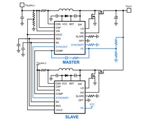
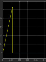
I added the initial condition in simscape, and try to simulate on SIMULINK the webench simulation of this component, this is the circuit in webench:
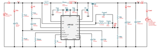
I add the circuit near the LM5122 manually in simscape. And my simulation doesn't work (it just pass through the DC VIN to VOUT ex. 12V as Vin 12 V as Vout ). Is there a way to import the all circuit in simscape without adding manually all the components?
Can you help me importing this model correctly?
Thanks.
Alessandro