This thread has been locked.

If you have a related question, please click the "Ask a related question" button in the top right corner. The newly created question will be automatically linked to this question.

DRV2700: DRV2700

Part Number: DRV2700
Other Parts Discussed in Thread: TINA-TI

Tool/software:

We are attempting to drive a haptic actuator. VD is at 5 volts. The amplifier seems to be attenuating the signal rather than amplifying, on top of that there is a notch at around 200 hz. I am drawing my signal from laptop Aux out. Cin was chosen based on the input impedance of the Amp to give a filter roll off at 15hz. The boost section seems to be working fine, voltage accross CBoost a good 103 as intended. From the internal schematic of the IC I cannot understand what's going wrong if the boost section is fine. We also tried with Ren as 10k to set enable only after powering the chip, that did not change much. 

I wonder if there's any trouble with the batch of ICs we have, we tried it out with 3 different boards, the one of them was overheating under no input, the other two were exhibiting notching and attenuation. Could any process during manufacturing the PCBs have damaged the IC? 

  • Hello, 

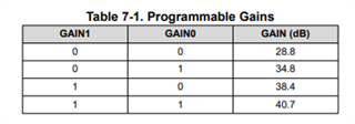
    Thank you for reaching out. What do you have your gain pins set to? For the max gain, they should both be pulled up. Could you provide scope screenshots of the output?

    First lets try to rule out some of the common issues.

    Is the inductor saturation current properly rated for the current limit set by Rrext (the programmed current-limit must be less than the rated saturation limit of the inductor)?

    Is the boost capacitor rated for the boost voltage? 

    What is the capacitance of your load? 

    Is the thermal pad of the DRV2700 device soldered directly to the thermal pad on the PCB? The thermal pad of the PCB must be connected to the ground net with thermal vias to any existing backside or internal copper ground planes. 

    Regards,
    Sydney Northcutt 

  • output at 250 hz, 0.5 V p-p input

    Thanks for the response here are the details. I had gain set to 0,0 to start with but it doesn't look like changing that does anything to the output. 

    Inductor saturation current = 2.7 A> I_lim = 2.32

    CBoost is rated at 250V

    Thermal pads look good, there is no noticeable heating on the two devices that have good CBoost voltage. 

    CLoad is 3uF but there is no good output even with the load disconnected. 

    The design is basically identitical to the Eval board which works perfectly. The following changes were made

    - I pulled out the input filters, as they were for PWM, and that was recommended for inputting an analog signal from a DAC.

    - Added the RC circuit to the Enable input

    - Chose Rfb1 and Rfb2 to get the right boost voltage (we know that worked)

    All other components connected to the driver are the same as on the Eval board. I wanted to stay with what I knew worked.

  • Hi, 

    I see. The schematic looks good and the ratings are correct. Could you provide the layout files for us to examine? If so, feel free to post here or email the files. Maybe something there is the issue here.

    Regards,
    Sydney Northcutt 

  • Hi Sydney

    Pl find encl. the layout file PDF (created using PADS software)G244_DRIVER SAARAS.pdf

    The entire layout files can be accessed here.https://1drv.ms/f/c/450e2df3dfa5ebbf/EvMO6NZZS8FHl4v-225Aa-4BOBwrIJm6zpM7RegfgLn0Yg?e=6sumWy

    regards

  • Hello, 

    Thank you for providing the files. Please allow a few days for us to review. 

    Regards,
    Sydney Northcutt 

  • Hi, 

    I am having trouble opening the full layout files, can you share them another way? I can send you an email to start a thread. 

    Regards,
    Sydney Northcutt 

  • Hi

    Had uploaded the layout files on the share provided over email (27th June). Pl review 

    regards

  • Hello, 

    Apologies for the delay here. There are a few things that could be optimized, but I don't notice anything that would cause the reported issues in the layout. To clarify, you have a total of three boards, two of which do not have the correct output and one that is overheating, correct? Are you able to tell if the device itself is heating or the external componentry? 

    I think we should debug the two semi-working boards first. Once we have two boards working we can swap the DRV2700 devices between a working and non working board so we can determine if it is the device or the board / external componentry that is causing the heating. 

    On the two semi-working boards, could you measure the pins below on the scope? One screen shot without any input to IN+/- and then another with the input signal applied would be great.
    - PVDD
    - EN (after resistor)
    - IN+ 
    - OUT+ 

    Regards,
    Sydney Northcutt 

  • Hi

    The basic DRV2700 model is not behaving as expected.  I must be missing something quite obvious, but I am at a loss.  Could you please forward the attached TINA-TI simulation file to the relevant TI folks with the following question:  "V_fb is not outputting the expected 1.3V in the transient analysis, instead settling to ~60mV, thus the boost voltage is far lower than expected.  Could you please enlighten me on what I am missing in this basic AC-coupled design?"  Thanks.Driver sim.TSC

  • Hello, 

    Opening and running your project, I saw the same output as you. Using the same passive components copied into a previous DRV2700 project, I see the correct output. It seems the simulation parameters for DRV700 are either not downloading or loading correctly. Can you try the below project file? 

    0407.DRV2700.TSC

    Regards,
    Sydney Northcutt