


Tool/software:
Husqvarna have now made their first prototypes with our DRVs and they have a questions on rise and fall time adjustments for the DRV8329, please see question below.
Can you please have a look ?
Mail 1
Hello,
We are now testing out the MCBT10 and there is an issue that I don’t really understand when using the DRV8329 gate driver,
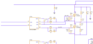
I would like to change the rise and fall time in this application. With current values I have a rise time of 12 to 18ns and fall time of 30 to 45ns depending on the power FET brand we are using.
I’m aiming for 50ns for both rise and fall time and for that reason I changed R701 and R702 to 200ohm and R704 and R705 to 58ohm. (For all three phases)
After changing values I got a rise time of 44ns (12ns before) and fall time 107ns!!!(35ns before).
Is this what I can expect? If so why? Is there a better way to change the rise and fall time. (Maybe add capacitors instead of/in parallel with R735 and R736?
 MCACD30N04HE3_PDFN5060_8D_-3365684.pdf
Mail 2
I looked at it (chapter 9.2.1.1.3 Gate Drive Current and 9.2.1.1.4 Gate Resistor Selection) , and it was pretty much true. (At first I didn’t know what time I needed.) It is right for the high side, but not for the low side. There the times are much longer. You can understand this considering that the high side loads with VDD+ bootstrap voltage which in my case is around 33V while the low side only loads with about 13V why the low side flank is about 3 times longer than the high side. This is very true of my measurements.
With 51ohm positive flank =12ns negative flank = 36ns
When I then test with 120ohm to high side and 75ohm on the negative side so became positive flank =36ns negative flank = 73ns which can be reasonable.
The goal is about 50 ns on both positive and negative, which is why I am changing again.
200ohm to high side and 58ohm to negative which results in positive flank =46ns which was my goal but negative flank = 107ns which I do not understand. I have double checked the resistance values and the positions values and they are correct.
The transistor I use requires relatively little charge to get started.
Total Gate charge QG 23
Gate-Source charge Qgs 3.5
Gate-drain charge Qgd 6.5
Could it be that we are experiencing phenomena because the gate currents are too low?
Attach data sheet to transistor.
