Tool/software:
Hey BLDC team,
I have a customer working with the DRV8353FSRTAR for a new project and there are a couple of items in the datasheet that we're hoping you can help provide clarity on:
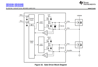
- There are many various grounds mentioned throughout the datasheet (i.e. GND, AGND, PGND, BGND, & DGND). Can you please help to clarify what all of the grounds signify and whether any specific precautions should be taken in order to ensure a stable ground for this device? The only signals actually routed out to pins seem to be GND and AGND so are the other signals purely internal ground nets?
- The datasheet also mentions "In sleep mode and when VVM < VUVLO, all external MOSFETs are disabled. The high-side gate pins, GHx, are pulled to the SHx pin by an internal resistor and the low-side gate pins, GLx, are pulled to the PGND pin by an internal resistor". Can you please share the value of these internal resistors as I don't think this is specified in the datasheet?
-Matt Calvo