This thread has been locked.

If you have a related question, please click the "Ask a related question" button in the top right corner. The newly created question will be automatically linked to this question.

MCF8316A: MCF8316A1VRGFR: Documents on programming this device

Part Number: MCF8316A
Other Parts Discussed in Thread: MSP430FR2355,

Tool/software:

I am a Device Support Engineer from BPM. We have a customer who needs this device 'MCF8316A1VRGFR' supported with our programmer. We see that their data file is in .json format. Can you provide us with a programming guide for this device. Thanks!

  • Hi Vigita,

    Please refer to the MCF8316A Datasheet section 7.6 EEPROM access and I2C interface for details on how to program the EEPROM using its I2C interface protocol.

    We also have this E2E FAQ, which provides an example firmware project that uses the MSP430FR2355 LaunchPad to program the EEPROM on a MCF8316A.

    Regards,
    Eric C.

  • I see. Thanks!. I will try and will get back to you

  • Hi Vigita,

    No problem! Please let me know if you have any questions with the provided information above.

    Regards,
    Eric C.

  • What is the slave I2C address for this device. Can you provide us the power on conditions needed for just writing EEPROM using I2C

  • Hi Vigita,

    The default I2C target address is 0x01 for the MCF8316A. However, this can be configured to a different value by writing into EEPROM.

    Ensure FG and nFAULT pins have pull-ups to 3.3~5V, otherwise, the device won't power-up normally. No SPEED input command should be provided. The device should power-on into MOTOR_IDLE state. 

    Regards,
    Eric C.

  • Hi Eric,

    I am having some doubts regarding the data file of this device.

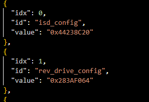
    The customer has shared a data file in .json format. I am having some doubts in the data file. 
    As per specs, this device has 4 sets of configuration registers. For example, let's say, we need to program the ISD configuration, then the right address register to store the value will be 80h. And for Reverse Drive configuration, it will be 82h.
     
    I see in the data file, it is Id = 0. It starts from 0 for each set of registers
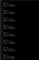
    And there are some registers in the data file that I do not see in the datasheet. They are
    Can you confirm us, if this in fact how the data file will be. If so, can you tell us how we can program the device, if the register addresses are not mentioned in the data file? Thanks!
  • Hi Vigita,

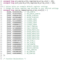
    The example programming code linked in E2E FAQ for the MSP430FR2355 LaunchPad to program the EEPROM does not read a .json file. The example code uses the values in an array which needs the desired register values to be manually input.

    The .json files with the register configuration are used with our GUIs such as Motor Studio. The idx in the .json is used to indicate the values position in the register map for the Motor Studio GUI when the GUI loads the register values into the GUI.

    there are some registers in the data file that I do not see in the datasheet

    all ana_trim registers are reserved registers, this is why they are not mentioned in the datasheet. These registers should not be written to, the array in the example code contains all the registers required to program the device so it operates as desired.

    Regards,

    Joshua

  • Hi Joshua,

    I would like to know how the data file is supposed to be? A .csv or .text, or something else. I assume the data file should have the register address, and the value to be written to that address. Can you provide us with a sample data file. That would be really helpful. Thanks!

  • Hi Vigita,

    Can I get more information about your programming set up?

    After further reviewing the screenshots you provided of the .json file, this appears to be an older format of the .json used with our old GUI on dev.ti.com. These old GUIs where device specific which is why addresses were not included in the .json.

    If you are using Motor Studio and a MCF8316AEVM, then the file type to use is a .json file like the one below:

    {
    "signature":"oneui-register-data",
    "data":[
    [
    {
    "idx":0,
    "id":"ISD_CONFIG",
    "value":"0x6C230C3C",
    "addr":"0x00000080"
    },
    {
    "idx":1,
    "id":"REV_DRIVE_CONFIG",
    "value":"0xA8200000",
    "addr":"0x00000082"
    },
    {
    "idx":2,
    "id":"MOTOR_STARTUP1",
    "value":"0x6568C700",
    "addr":"0x00000084"
    },
    {
    "idx":3,
    "id":"MOTOR_STARTUP2",
    "value":"0x9A82200D",
    "addr":"0x00000086"
    },
    {
    "idx":4,
    "id":"CLOSED_LOOP1",
    "value":"0x0E3191BD",
    "addr":"0x00000088"
    },
    {
    "idx":5,
    "id":"CLOSED_LOOP2",
    "value":"0x99E59091",
    "addr":"0x0000008A"
    },
    {
    "idx":6,
    "id":"CLOSED_LOOP3",
    "value":"0x30800002",
    "addr":"0x0000008C"
    },
    {
    "idx":7,
    "id":"CLOSED_LOOP4",
    "value":"0x298A84B0",
    "addr":"0x0000008E"
    },
    {
    "idx":8,
    "id":"REF_PROFILES1",
    "value":"0x00000000",
    "addr":"0x00000094"
    },
    {
    "idx":9,
    "id":"REF_PROFILES2",
    "value":"0x00000000",
    "addr":"0x00000096"
    },
    {
    "idx":10,
    "id":"REF_PROFILES3",
    "value":"0x00000000",
    "addr":"0x00000098"
    },
    {
    "idx":11,
    "id":"REF_PROFILES4",
    "value":"0x00000000",
    "addr":"0x0000009A"
    },
    {
    "idx":12,
    "id":"REF_PROFILES5",
    "value":"0x00000000",
    "addr":"0x0000009C"
    },
    {
    "idx":13,
    "id":"REF_PROFILES6",
    "value":"0x00000000",
    "addr":"0x0000009E"
    }
    ],
    [
    {
    "idx":0,
    "id":"FAULT_CONFIG1",
    "value":"0xA6EA4326",
    "addr":"0x00000090"
    },
    {
    "idx":1,
    "id":"FAULT_CONFIG2",
    "value":"0xFF0220B8",
    "addr":"0x00000092"
    }
    ],
    [
    {
    "idx":0,
    "id":"INT_ALGO_1",
    "value":"0xA43141BD",
    "addr":"0x000000A0"
    },
    {
    "idx":1,
    "id":"INT_ALGO_2",
    "value":"0x000001A3",
    "addr":"0x000000A2"
    }
    ],
    [
    {
    "idx":0,
    "id":"PIN_CONFIG",
    "value":"0x08000000",
    "addr":"0x000000A4"
    },
    {
    "idx":1,
    "id":"DEVICE_CONFIG1",
    "value":"0x00101465",
    "addr":"0x000000A6"
    },
    {
    "idx":2,
    "id":"DEVICE_CONFIG2",
    "value":"0xC0003107",
    "addr":"0x000000A8"
    },
    {
    "idx":3,
    "id":"PERI_CONFIG1",
    "value":"0x81E81F00",
    "addr":"0x000000AA"
    },
    {
    "idx":4,
    "id":"GD_CONFIG1",
    "value":"0x00000000",
    "addr":"0x000000AC"
    },
    {
    "idx":5,
    "id":"GD_CONFIG2",
    "value":"0x00000000",
    "addr":"0x000000AE"
    }
    ],
    [
    {
    "idx":0,
    "id":"GATE_DRIVER_FAULT_STATUS",
    "value":"0x00000000",
    "addr":"0x000000E0"
    },
    {
    "idx":1,
    "id":"CONTROLLER_FAULT_STATUS",
    "value":"0x00000000",
    "addr":"0x000000E2"
    }
    ],
    [
    {
    "idx":0,
    "id":"ALGO_STATUS",
    "value":"0x27A60004",
    "addr":"0x000000E4"
    },
    {
    "idx":1,
    "id":"MTR_PARAMS",
    "value":"0x90619100",
    "addr":"0x000000E6"
    },
    {
    "idx":2,
    "id":"ALGO_STATUS_MPET",
    "value":"0xE1000000",
    "addr":"0x000000E8"
    }
    ],
    [
    {
    "idx":0,
    "id":"ALGO_CTRL1",
    "value":"0x00000000",
    "addr":"0x000000EA"
    }
    ],
    [
    {
    "idx":0,
    "id":"ALGO_DEBUG1",
    "value":"0x80000000",
    "addr":"0x000000EC"
    },
    {
    "idx":1,
    "id":"ALGO_DEBUG2",
    "value":"0x00000000",
    "addr":"0x000000EE"
    },
    {
    "idx":2,
    "id":"CURRENT_PI",
    "value":"0x012D012E",
    "addr":"0x000000F0"
    },
    {
    "idx":3,
    "id":"SPEED_PI",
    "value":"0x022A012A",
    "addr":"0x000000F2"
    },
    {
    "idx":4,
    "id":"DAC_1",
    "value":"0x00000000",
    "addr":"0x000000F4"
    },
    {
    "idx":5,
    "id":"DAC_2",
    "value":"0x00000000",
    "addr":"0x000000F6"
    }
    ],
    [
    {
    "idx":0,
    "id":"ALGORITHM_STATE",
    "value":"0x00000000",
    "addr":"0x00000190"
    },
    {
    "idx":1,
    "id":"FG_SPEED_FDBK",
    "value":"0x0400EC20",
    "addr":"0x00000196"
    },
    {
    "idx":2,
    "id":"BUS_CURRENT",
    "value":"0x00000000",
    "addr":"0x00000410"
    },
    {
    "idx":3,
    "id":"PHASE_CURRENT_A",
    "value":"0x000A0000",
    "addr":"0x00000440"
    },
    {
    "idx":4,
    "id":"PHASE_CURRENT_B",
    "value":"0xFFFA0000",
    "addr":"0x00000442"
    },
    {
    "idx":5,
    "id":"PHASE_CURRENT_C",
    "value":"0x00000000",
    "addr":"0x00000444"
    },
    {
    "idx":6,
    "id":"CSA_GAIN_FEEDBACK",
    "value":"0x00000003",
    "addr":"0x00000468"
    },
    {
    "idx":7,
    "id":"VOLTAGE_GAIN_FEEDBACK",
    "value":"0x00000002",
    "addr":"0x00000472"
    },
    {
    "idx":8,
    "id":"VM_VOLTAGE",
    "value":"0x00000000",
    "addr":"0x00000476"
    },
    {
    "idx":9,
    "id":"PHASE_VOLTAGE_VA",
    "value":"0x0000376C",
    "addr":"0x0000047A"
    },
    {
    "idx":10,
    "id":"PHASE_VOLTAGE_VB",
    "value":"0x0000376C",
    "addr":"0x0000047C"
    },
    {
    "idx":11,
    "id":"PHASE_VOLTAGE_VC",
    "value":"0x0001F2D4",
    "addr":"0x0000047E"
    },
    {
    "idx":12,
    "id":"SIN_COMMUTATION_ANGLE",
    "value":"0x07E7B288",
    "addr":"0x000004B6"
    },
    {
    "idx":13,
    "id":"COS_COMMUTATION_ANGLE",
    "value":"0x0128ADF9",
    "addr":"0x000004B8"
    },
    {
    "idx":14,
    "id":"IALPHA",
    "value":"0x000A8000",
    "addr":"0x000004D2"
    },
    {
    "idx":15,
    "id":"IBETA",
    "value":"0x0054DED8",
    "addr":"0x000004D4"
    },
    {
    "idx":16,
    "id":"VALPHA",
    "value":"0xFF83F708",
    "addr":"0x000004D6"
    },
    {
    "idx":17,
    "id":"VBETA",
    "value":"0x000EE48C",
    "addr":"0x000004D8"
    },
    {
    "idx":18,
    "id":"ID",
    "value":"0x00556269",
    "addr":"0x000004E2"
    },
    {
    "idx":19,
    "id":"IQ",
    "value":"0x0001EB50",
    "addr":"0x000004E4"
    },
    {
    "idx":20,
    "id":"VD",
    "value":"0xFFFCBD4D",
    "addr":"0x000004E6"
    },
    {
    "idx":21,
    "id":"VQ",
    "value":"0x007D0BEC",
    "addr":"0x000004E8"
    },
    {
    "idx":22,
    "id":"IQ_REF_ROTOR_ALIGN",
    "value":"0x00000000",
    "addr":"0x00000524"
    },
    {
    "idx":23,
    "id":"SPEED_REF_OPEN_LOOP",
    "value":"0x00000000",
    "addr":"0x0000053C"
    },
    {
    "idx":24,
    "id":"IQ_REF_OPEN_LOOP",
    "value":"0x0CCC9C80",
    "addr":"0x0000054C"
    },
    {
    "idx":25,
    "id":"SPEED_REF_CLOSED_LOOP",
    "value":"0x00000000",
    "addr":"0x000005D4"
    },
    {
    "idx":26,
    "id":"ID_REF_CLOSED_LOOP",
    "value":"0x00000000",
    "addr":"0x00000606"
    },
    {
    "idx":27,
    "id":"IQ_REF_CLOSED_LOOP",
    "value":"0x00000000",
    "addr":"0x00000608"
    },
    {
    "idx":28,
    "id":"ISD_STATE",
    "value":"0x00000000",
    "addr":"0x00000682"
    },
    {
    "idx":29,
    "id":"ISD_SPEED",
    "value":"0x00000000",
    "addr":"0x0000068C"
    },
    {
    "idx":30,
    "id":"IPD_STATE",
    "value":"0x00000000",
    "addr":"0x000006C0"
    },
    {
    "idx":31,
    "id":"IPD_ANGLE",
    "value":"0x00000000",
    "addr":"0x00000704"
    },
    {
    "idx":32,
    "id":"ED",
    "value":"0x00000000",
    "addr":"0x0000074A"
    },
    {
    "idx":33,
    "id":"EQ",
    "value":"0x00000000",
    "addr":"0x0000074C"
    },
    {
    "idx":34,
    "id":"SPEED_FDBK",
    "value":"0x00000000",
    "addr":"0x0000075A"
    },
    {
    "idx":35,
    "id":"THETA_EST",
    "value":"0x00000000",
    "addr":"0x0000075E"
    }
    ]
    ]
    }

    If you will be using the example CCS project in the Program MCx BLDC motor driver through I2C using MSP430 LaunchPad FAQ then the register map needs to be manually written in to the array in the main.c file in the CCS project.

    Motor Studio also has the ability to output the register configuration in a .csv format, although this file type is not used by Motor Studio or the CCS project:

    Default MCF8316C Register Config.csv

    Regards,

    Joshua

  • Is there anything else for powering the device. I provides 5v to VM pins (pin numbers: 9 10 and 11). FG and nFault pins are pulled up. Yet, the device is not responding to the slave address. Am I missing something?

  • Hi Vigita,

    To check if the device is powering up correctly, can you check if AVDD = 3.3V and DVDD = 1.5V after 5V is applied to VM? If these voltages are not outputting the correct voltage, check the amount of current that is being drawn from the power supply.

    If the nFAULT and FG pins are being pulled up by an external power supply (not from AVDD or 3.3v from the integrated buck) then please make sure these pins are pulled up before powering the device or the MCF8316A may enter a test mode where I2C communication will no longer work.

    Regards,

    Joshua

  • Hi Joshua,

    So this is my power on conditions. I float the clock and data pins. Then I set VPU to 3.6v, so that the FG and Fault pin is pulled up to 3.6. Then I applied 5v to VM pins. After that, i tried communicating with the device, the device did not respond to any address.

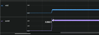
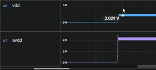
    I measured voltage from avdd and vdd pins. For 5V supply, the voltage on avdd and dvvd pins are 695mv and 660mv. I do not think the device is getting powered on at 5v. 

    Then I increased the voltage to 12v. And still not able to communicate with the device. For 12V supply, the voltage on avdd and dvvd pins are 4.06v and 2v

    Am i missing something? Do sda and scl pins need external pull ups?

  • Hi Vigita,

    AVDD and DVDD are outputting values greater than their Abs Max values. This could indicate that the MCF8316A has become damaged but it could also be due to the measurement method used. 

    If you are able to, can you try measuring the AVDD and DVDD voltages of another MCF8316A device?

    Do sda and scl pins need external pull ups?

    We recommend using a pull-up resistor value of 5.1 kOhms on SDA and SCL to make sure these pins can be read as logic high.

    Can you measure SDA and SCL to check if the voltage goes above 0.65 * AVDD while logic high? If the logic high voltage is not getting above 0.65 * AVDD then the MCF8316A cannot register a logic high input. 

    Regards,

    Joshua

  • The speed pin in grounded. Will that affect communicaition?

  • Grounding the speed pin will only if DEV_MODE is set to 1b so that the device can go into sleep mode. In sleep mode, AVDD and the I2C bus are disabled so I do not think this is the cause since when applying 12V to VM you were able to measure AVDD as going above 3.3V

    Please do try try measuring the AVDD and DVDD voltages of another MCF8316A device seeing these voltages being measured as outputting a voltage above their abs max ratings could indicate damage which may be the cause of the communications issues.

    If you would like, I can review the schematic to check for anything which could be an issue.

    Regards,

    Joshua

  • On a different sample

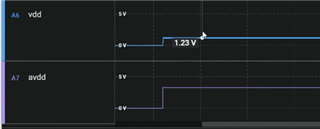
    we get 1.23v on dvdd pin

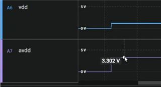
    and 3.3v on avdd

    The device does not acknowledge back when I send the slave address (0x01), and write bit 0

  • Hi Vigita,

    Thank you for checking the AVDD and DVDD of another MCF8316A, this helped to confirm the communication issue was not caused by damage to the device.

    Can you provide the following:

    1. Your schematic

    2. A capture of the SDO and SCL when attempting to communicate with the MCF8316A

    Regards,

    Joshua

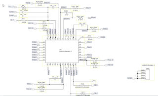
  • This is the schematics

  • The resistors connected to SDA and SCL pins are 51.1k

  • Hi Vigita,

    I will need to reach out to my team about this question. I aim to get back with you by next Wednesday.

    Regards,

    Joshua

  • Hi Vigita,

    Sorry for the delay in reply.

    1. Have you been able to communicate with the MCF8316A at any point? If you have been able to communicate before, did you write to EEPROM?
    2. Can you try all the I2C target address to check if the EEPROM had a non-default I2C address programmed?
    3. The MCF8316A has errata regarding the I2C communication. We recommend customers switch to the MCF8316C if possible since this device as updated firmware to fix many of the errata. The MCF8316C is pin-to-pin with the MCF8316A.

    Regards,

    Joshua

  • Hi Joshua,

    We resolved the problem.

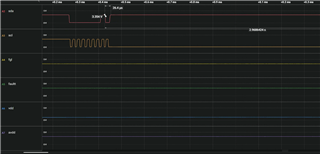
    You had previously informed that if the device powers up correctly, it will output 3.3v at avdd pin and 1.5v at dvdd pin. When we gave 5v to VM pin, we got 3.3v at avdd pin, but at dvdd pin, we got only 1.2v. I have shared the waveforms previously. We went through the specs again and saw that for dvdd pin to output 1.5, the FB_BK pin should be given 3.3v. Once we gave 3.3v to FB_BK, the dvdd pin output 1.5v and the device gave ack for the correct I2C address.

    We were able to program the device after that.

  • I am glad that you were able to discover the cause of the issue! I do regret that I did not immediately notice that DVDD regulators output was below the spec. Just to provide a bit of context, the DVDD regulator is used to power the digital core within the MCF8316A so this voltage not being within spec was leading to the I2C peripheral not turning on.

    Regards,

    Joshua