This thread has been locked.

If you have a related question, please click the "Ask a related question" button in the top right corner. The newly created question will be automatically linked to this question.

DRV8705-Q1: DRV8705-Q1

Part Number: DRV8705-Q1

Tool/software:

Hi team,

I have a few questions about DRV8705-Q1:

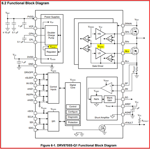
I use the DRV8705-Q1 in hardware mode, as a set of bridge drive outputs

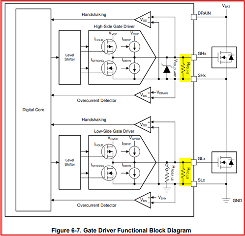
1.The GHx of the high-side switch is powered by the GLx by raising the voltage through a charge pump,Then, when the high-side switch is not turned on, who provides the electricity for the high-side switch GLx?

2.What is the voltage of GHx and GLx when the high side switch is not driven? Why?

3.When a short power failure occurs on the high side and a short power failure occurs on the low side, the chip will shut down the output due to VDS overcurrent detection. However, since the VDS overcurrent mode is fixed to cycle by cycle on the hardware device model, the fault bit will be cleared and the output will be retried, resulting in a negative pressure of -10V on SHx. Can this negative pressure chip withstand it?

4.In response to problem 3, I added the strategy of detecting that the nFAULT is low, judging that the chip is faulty, and then turning off the output. The program is refreshed every 100ms. Before the output is turned off by the software, I can see that the nFAULT pin of the chip constantly changes between high and low, which is not a stable state. The chip is still resetting nFAULT, is this strategy OK?

5.In cycle by cycle mode, after detecting an overcurrent event, the nFAULT will be set and the next PWM input will clear the nFAULT register bit, but I found in the actual test that the PWM has not input the nFAULT register bit is cleared, what is the reason?(The blue line is the high side switch output short ground, and the pink line is the nFAULT pin)

Hope to receive your reply, thank you~

  • Hello,

    Please allow me 24 hours to look into these questions and provide feedback. 

    Best,

    David

  • Hello, 

    1. When the high-side switch is not turned on GLx gets voltage from GVDD.

    2. When the high side switch is not driven, the GHx and GLx have pull-down resistors making GHx = SHx and GLx = GND.

    3. On the H/W device variants the VDS overcurrent mode is fixed to cycle by cycle and tVDS_DG is fixed to 4 µs. Meaning if overcurrent (short) occurs the outputs (SHx) will be disabled and checked every 4us until the fault clears. 

    4. The nFAULT pin will be driven low in the event of VDS overcurrent, no code is required. 

    5. If possible, could you please describe how you are running the short test? Are you using a wire to short SH1 and SH2 together, or SHx to GND?

    Best,

    David

  • Hello David, 

    On the first question, Who powers the SHx and what is the flow of charge pump between SHx and GHx once powered on?

    On the fourth question, the nFAULT pin will be driven low in the event of VDS overcurrent. However, when the short circuit fault still exists, it will always clear the fault bit, as shown in the figure. Shouldn't you keep the nFAULT low until the fault disappears?

    On the fifth question, When driving the 8705 forward turn, I used a wire to short the SHx to the ground.

    Best,

    Jie

  • Hi Jie,

    On the first question, Who powers the SHx and what is the flow of charge pump between SHx and GHx once powered on?

    The charge pump allows the high-side gate drivers to properly bias the external N-channel MOSFET with respect to its source voltage across a wide input supply voltage range.

    The figures in the datasheet and the ones posted above, can help to show how the VCP is used to bias the HS FET, and powered by PVDD. 

    On the fourth question, the nFAULT pin will be driven low in the event of VDS overcurrent. However, when the short circuit fault still exists, it will always clear the fault bit, as shown in the figure. Shouldn't you keep the nFAULT low until the fault disappears?

    This appears to be behaving as intended. The cycle-by-cycle mode will keep re-enabling the outputs and nFAULT high and keep checking if the fault is there. In the Latched Fault Mode the device will behave as you described, nFAULT going low after fault detected and staying low until the fault is cleared with CLR_FLT. Unfortunately, the hardware varied is fixed to cycle by cycle mode with a 4us deglitch time. 

    The SPI version of this device would allow you to enter the Latched Fault Mode. 

    https://www.ti.com/tool/DRV8705S-Q1EVM 

    Best,

    David

  • Hello David, 

    I understood everything you said except for one question.According to the Gate Driver functional Block Diagram, the high-side GHx is driven by VCP, and the SHx is in a floating state. How can the high-side MOS be opened?

    Best,

    Jie

  • Hi Jie,

    The purpose of the charge pump is to supply the GHx pin with a higher voltage than SHx. When turning on the FET, the GHx pin should be approximately   VM + 10V.

    Please see abs max and recommended values in the datasheet to verify and test on EVM.

    What value are you seeing at the GHx pin when turning on the FET?

    Best,

    David

  • Hello David, 

    When the FET is not turned on,who supplies the electricity to the SHx?

  • Hi Jie,

    This would depend on the control mode (PH/EN, PWM, Independent 1/2 Bridge) and input signals. The control tables in the datasheet help to show what is expected. 


    Best,

    David

  • Hello David,

    According to the internal block diagram of the charge pump, charging the capacitor through the switching MOSFETs makes the VCP approximately 10V higher than the PVDD.

    The purpose of the charge pump is to supply the GHx pin with a higher voltage than SHx. When turning on the FET, the GHx pin should be approximately   VM + 10V.When output, high side GHx is supplied by charge pump voltage VCP, GLx is supplied by PVDD?

  • Hi Jie,

    GLx is supplied by VGVDD. The voltage from GLx to SHx is around 11.25V at maximum when the low-side FET is on. 

    Best,

    David

  • Hello David,

    Sorry, I typed the wrong question.The purpose of the charge pump is to supply the GHx pin with a higher voltage than SHx. When turning on the FET, the GHx pin should be approximately   VM + 10V.When output, high side GHx is supplied by charge pump voltage VCP, SHx is supplied by PVDD?

    Best,

    Jie

  • Hi Jie,

    Yes, that is correct.

    Best,

    David