Tool/software:
Dear Sir/Madam,
I would like to control a dual speed wiper motor and am looking at using the DRV8702D-Q1.
There will be one DRV8702D-Q1 for each speed.
I am a little confused how to control DRV8702D-Q1.
I need to do the following:
* Turn the motor on
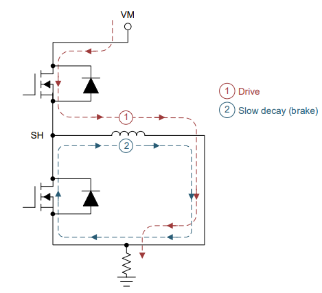
* Turn the motor off quickly (brake).
* Protect DRV8702D-Q1 from induced voltage into low-speed winding.
Simple as possible minimal control pin interface.
Hoping to just use IN1 and IN2 if possible and tie nSLEEP to 1.
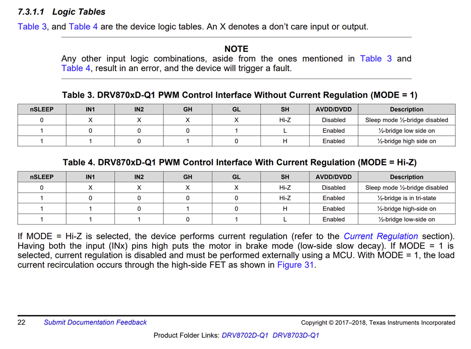
Q1. Do I use MODE =0 or MODE=1
Q2. Can I drive IN1 and IN2 with static DC values or do they need to be PWM controlled?
The following is the sequence I believe.
1. tri-state (motor is off) IN1=0 (high side off), IN2=0 (low side off)
2. turn on motor IN1=1 (high side on), IN2=0 (low side off).
3. wait until instructed to turn off.
4. turn off motor IN1=1 (high side on), IN2=1 (low side on) brake
5. tri-state (motor is off) IN1=0 (high side off), IN2=0 (low side off)
How long do you need to wait at step 4 before going to step 5.
Q3. If voltage is induced into motor winding do I turn off lower and upper FETs?
I understand that I will need to block current flowing into upper FET and also protect SH pin.
The following is the sequence I believe.
1. tri-state (motor is off) IN1=0 (high side off), IN2=0 (low side off)
Regards Joe