This thread has been locked.

If you have a related question, please click the "Ask a related question" button in the top right corner. The newly created question will be automatically linked to this question.

DRV8426: DRV8426PWPR misbehavior in power recycle

Part Number: DRV8426

Tool/software:

Hi, 

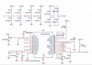
Please find the below schematic for DRV8426

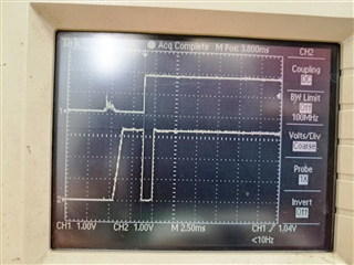
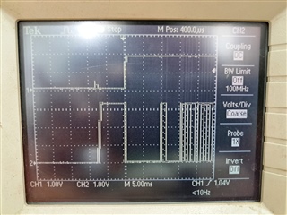
sometimes, during power recycle it gets trapped in improper condition,

where we can observe toggling in "fault" pin & similar activity can be observed on winding output pins (on very few instances, it get recover from this situation, without any intervention----by sending low signal on enable/ nSLEEP pin )

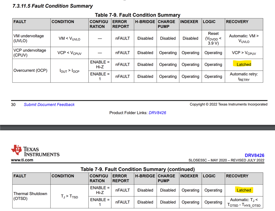
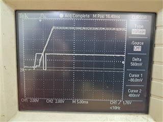
below are the images for enable pin & fault pin (in normal & problematic condition)

apart from above, it works fine in 1/8 mode

what can be root cause & recommended solution for it, 

Regards,

  • Hello AG,

    Thank you for sharing the stepper driver schematic and posting your question in this forum. While it is okay to use a pull-up resistor for nSLEEP depending on the PCB layout it is possible to have some noise coupling on this pin with a 15 kΩ pull-up. You can try with a reduced value or even a 0 Ω jumper for this nSLEEP pull-up. 

    When you power cycle please clarify if both VM and VCC3.3 were cycled simultaneously or only VM was cycled? When power was cycled was enough time allowed for VM to fully discharge from the capacitors before turning on? We've not come across reports of such power cycling issues with this device thus far. Can you also capture the VM power cycling waveform along with these signals. 

    Only two faults OCP and OTSD that could be potentially latched and cause nFAULT = 0. So if we can rule out these there should be no other latched faults that'd required nSLEEP to be toggled to 0 and then 1.


    Regards, Murugavel 

  • Hi Murugavel,

    Thanks for reply,

    1. power cycling done through machine DC supply ON/OFF switch, so applicable for both motor voltage & 3.3V

    2. When power was cycled if we gave VM time to fully discharge and go down below 1V, then it works OK else it stuck in trap , please find the attached image for motor & fault pin in normal condition

  • Hi Murugavel,

    I have reduced value to 0 Ω jumper for this nSLEEP pull-up, but results are same

    Regards,

  • Hi AG,

    Thanks for doing the tests and sharing the details. 

    I have reduced value to 0 Ω jumper for this nSLEEP pull-up, but results are same

    This is good. nSLEEP VIH and VIL was already in compliance.

    1. power cycling done through machine DC supply ON/OFF switch, so applicable for both motor voltage & 3.3V

    The machine power supply system powering the DRV8426 may be having a very slow discharge profile (dV/dt) which is not ideal for digital POR (power on reset) circuits. 

    2. When power was cycled if we gave VM time to fully discharge and go down below 1V, then it works OK else it stuck in trap , please find the attached image for motor & fault pin in normal condition

    This is a typical signature of slow discharging power supply affecting POR behavior. As a fix to this issue in your system you can consider the following:

    1. Keep nSLEEP LOW at power on. Wait for a few milliseconds after power on and then wake up the device by nSLEEP HIGH. If this does not address the issue consider 2.

    2. If nSLEEP was HIGH during power on, issue an nSLEEP reset pulse a few milliseconds after power on. nSLEEP LOW for about 80 us after nSLEEP will reset the digital in the device. This will guarantee the device resets correctly regardless of slow dV/dt of the power supply.


    3. Improve the discharge rate dV/dt of the power supply when turned off. 1 and 2 should address the issue so this may not be necessary if everything else such as the MCU functions as expected in your system. 

    Thank you.

    Regards, Murugavel

  • Hi,

    If POR behaviour is only related to 3.3v, then it has faster dv/dt, which can be confirmed on waveforms

    Letme know, is there any h/w provision, by which we can achieve the same...as I do not have any mcu pin left for control

    Also suggest pin, voltage level rise and fall time, if I have to verify same in any particular pin

    Motor having bulk capacitance, so it is taking time to charge and discharge, what can be minimum capacitance value?

    Regards,

  • Hi AG,

    The POR behavior is related to VM. Minimum bulk capacitance depends on the trace distance from VM to power supply and motor current requirements. What is the current bulk capacitor value? I noticed 100 uF in your schematic. Is there anything in addition to it? What is the full-scale motor current IFS setting (VREF voltage)?

    Regards, Murugavel

  • Hi Murugavel,

    Thanks for confirmation, VREF is 1.2880

    as other few variable loads are also depend on the same line, reducing the bus capacitance seems difficult

    can you provide the POR range, rise time, fall time & trigger voltage values details need to be considered for VM, so I can try to adjust the same

    regards,

  • Hi AG,

    VREF is 1.2880

    So IFS will be about 585 mA. Would the stepper be energized while turning off the power? This could discharge the capacitor faster. We do not have rise time and file time specifications unfortunately. With a large capacitor we expect a slower dv/dt anyways. VRESET on VM would be about 3.9 V perhaps between 3 and 3.9 V. With your power supply in your application could you please monitor how much time it takes for VM to drop to 3 V after switching off the power? 

    Regards, Murugavel 

  • Hi Murugavel,

    It's very unfortunate that required data is not available in TI technical documents

    I have confirmed the timings (8.2 V to 3V, required time , approx. 600ms),further dV/dt becomes more slower

    as mentioned earlier, even we allow VM to go down in condition 1V<VM<3V, still latch up situation occurs 

    request you to have more investigation at your end...

    Regards,

  • Hi Murugavel,

    it seems, CHIP not working as per datasheet, please refer below points from 

    7.3.11.1 VM Undervoltage Lockout (UVLO)
    If at any time the voltage on the VM pin falls below the UVLO-threshold voltage for the voltage supply, all
    the outputs are disabled, and the nFAULT pin is driven low. The charge pump is disabled in this condition.
    Normal operation resumes (motor-driver operation and nFAULT released) when the VM undervoltage condition
    is removed.

    ideally below VM= 4.1V, chip should shutdown & resume properly above 4.2V

  • Hi AG,

    I have confirmed the timings (8.2 V to 3V, required time , approx. 600ms),further dV/dt becomes more slower

    as mentioned earlier, even we allow VM to go down in condition 1V<VM<3V, still latch up situation occurs 

    request you to have more investigation at your end...

    I'll check and see if we could get you minimum dV/dt requirements. This may take a few days. For this I'll get back to you around middle of next week.

    ideally below VM= 4.1V, chip should shutdown & resume properly above 4.2V

    Yes, this is true as long as VM does not decrease below the reset voltage. Assuming this would be 3.9 V, that statement holds good as long as VM stays above 3.9 V. This has been verified to work.

    Regards, Murugavel