Tool/software:
Hi Team,
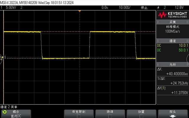
Previously, the DRV8323RS chip was used, with upper tube source/sink currents of 440mA and 380mA, and lower tube source/sink currents of 330mA and 280mA, respectively. It was used to drive a single MOS and has been mass-produced. The MOS gate driving waveform is normal, and the driving voltage remains at 11.375V. The waveform is as follows:
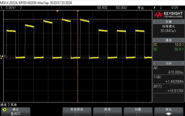
At present, a new project requires driving 2 MOSFETs, and we have adjusted the current output capability accordingly. The source/sink currents on the upper tube are 820mA and 740mA, respectively, and the source/sink currents on the lower tube are 680mA and 520mA, respectively. The MOS gate drive waveform is abnormal, jumping between 11.8 and 16.8V. The waveform is shown below.
Can you help analyze the cause?
note: There is no current limiting resistor added between the driver IC and the MOS transistor. In actual testing, if a 10 Ω resistor is added, the driving voltage will not jump, but the rise and fall time will change significantly.
Thx!