This thread has been locked.

If you have a related question, please click the "Ask a related question" button in the top right corner. The newly created question will be automatically linked to this question.

DRV8353: SPI Communication with Gate Driver

Part Number: DRV8353

Tool/software:

Dear TI Support Team,

I am working with the DRV8353RS gate driver and encountering difficulties with the SPI register read operation. The SPI write functions appear to be working correctly, but I am unable to read back valid data from the registers.

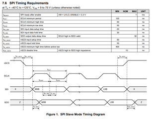
I have referred to Section 8.5.1.1.1 in the datasheet, particularly regarding the SDI input and SDO output word formats for SPI communication. For the read command:

I am setting the Read/Write bit (B15) to 1 to initiate the read.
The Address (A3–A0, bits B14–B11) is being set correctly, and I expect the data corresponding to the register to be returned in bits B10–B0 of the response.

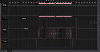
However, in practice, the MISO line (Channel 0 in the attached logic analyzer capture) consistently returns 0xFF, rather than the expected register values. The MOSI signal (Channel 1) shows that the correct command (e.g., 0x90 for register read) is being sent, and the SPI clock and enable signals (Channels 2 and 3) are operating as required.

I have tried writing 0x00 content to 0x40 register rather than 0xFF, which is also not working as expeted. 

Additionally, based on the datasheet, I understand that the first 5 bits of the response on the MISO line are "don't care" bits, but the following 11 bits (B10–B0) should contain the actual data from the register. This expected behavior is not occurring, and I am unsure what could be causing this mismatch.

Could you kindly provide guidance on any potential issues that could cause the SPI read operation to fail in this way? Any specific timing requirements or other configuration settings that might resolve this would be greatly appreciated.

Thank you for your support!

Best regards,
- Himavanth Reddy

  • Hi Himavanth,

    Is this type of response from SDO happening on ALL your register reads? Meaning any register you read the response is 0xFF? Is there a pull up resistor on SDO?

    are you following the SPI timing requirements?

    I have seen this kind of SDO response when users try and communicate to the device before tREADY

    Regards,

    Yara

  • Hi Yara,

    In reply to previous quetions, Yes, the 0xFF response is happening on all register reads. There is a 1K pull-up resistor on the SDO line.

    I’ve also checked the SPI timing requirements, and the clock high time (tclkH) is 375 ns, and the clock low time (tclkL) is 437 ns, which are within the specified limits.Additionally, I am ensuring that the tREADY time is respected by introducing a 50 ms delay before attempting to read, but the response is still the same.

    Do you have any further suggestions or potential areas to investigate?

    Thanks,
    Himavanth

  • Hi Himavanth,

    Can you please confirm VM > 10V, VDRAIN > 10V, and ENABLE is high (3.3V). Please also check that the part is ON by measuring DVDD voltage as 5.0V (this may seem very obvious but I want to politely confirm it since it was not asked in this thread). SPI does not respond when the part is unpowered or if ENABLE is low (sleep mode).

    Can you measure to see if there is a diode between GND and SDO line internal to the IC (you sould be able to use a digital multimeter to do this by placing + on GND and - on SDO line in diode test mode)? It should read 0.5-0.8V. The power can be turned off from the system for this test, but make sure MCU is not connected to SDO line. The SDO pull-down MOSFET has an internal body diode and if we cannot detect a diode here (DMM reads open) this tell us that the internal structure is damaged or if the SDO pin is not making contact to the PCB trace (cold solder joint, etc).

    You can take a look at Figure 40 (top of page 41) from the DRV835x datasheet for a picture of this diode structure on SDO.

    Regards,

    Yara